SE1002 Equivalente. Reemplazo. Hoja de especificaciones. Principales características
Número de Parte: SE1002
Material: Si
Polaridad de transistor: NPN
ESPECIFICACIONES MÁXIMAS
Disipación total del dispositivo (Pc): 0.2
W
Tensión colector-base (Vcb): 45
V
Tensión colector-emisor (Vce): 45
V
Tensión emisor-base (Veb): 4
V
Corriente del colector DC máxima (Ic): 0.1
A
Temperatura operativa máxima (Tj): 125
°C
CARACTERÍSTICAS ELÉCTRICAS
Transición de frecuencia (ft): 200
MHz
Capacitancia de salida (Cc): 4
pF
Ganancia de corriente contínua (hfe): 100
Paquete / Cubierta:
TO106
Búsqueda de reemplazo de SE1002
-
Selección ⓘ de transistores por parámetros
SE1002 PDF detailed specifications
0.1. Size:338K cn sino-ic
se100250gts.pdf 
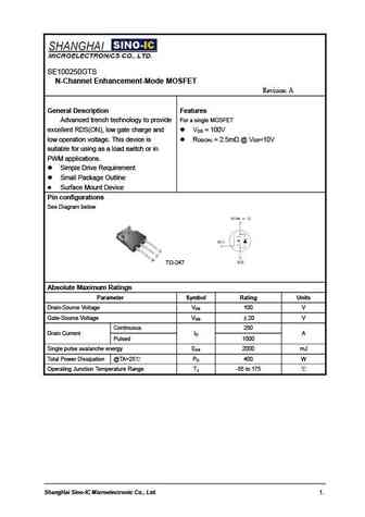
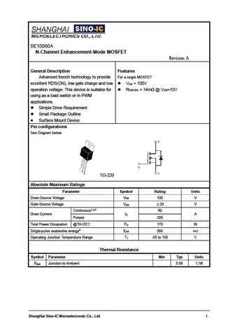
SE100250GTS N-Channel Enhancement-Mode MOSFET Revision A General Description Features For a single MOSFET Advanced trench technology to provide excellent RDS(ON), low gate charge and V = 100V DS low operation voltage. This device is R =2.5m @V =10V DS(ON) GS suitable for using as a load switch or in PWM applications. Simple Drive Requirement Small Package Outlin... See More ⇒
9.1. Size:624K cn sino-ic
se10080a.pdf
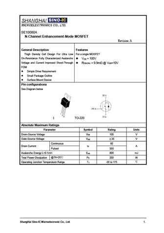
SE10080A N-Channel Enhancement-Mode MOSFET Revision A General Description Features Thigh Density Cell Design For Ultra Low For a single MOSFET On-Resistance Fully Characterized Avalanche V =100V DS Voltage and Current Improved Shoot-Through R =9.9m @V =10V DS(ON) GS FOM Simple Drive Requirement Small Package Outline Surface Mount Device Pin configurations ... See More ⇒
9.2. Size:358K cn sino-ic
se100p60.pdf
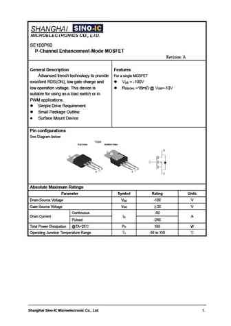
SE100P60 P-Channel Enhancement-Mode MOSFET Revision A General Description Features For a single MOSFET Advanced trench technology to provide excellent RDS(ON), low gate charge and V = -100V DS low operation voltage. This device is R =18m @V =-10V DS(ON) GS suitable for using as a load switch or in PWM applications. Simple Drive Requirement Small Package Outline ... See More ⇒
9.4. Size:470K cn sino-ic
se100150g.pdf
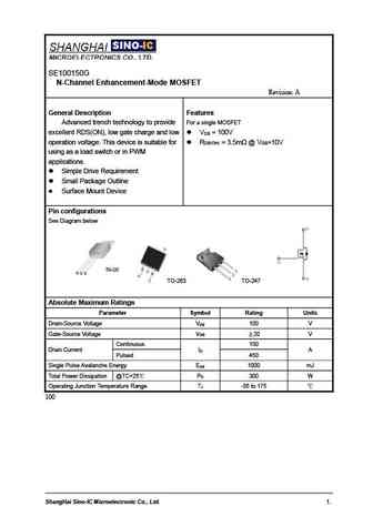
SE100150G N-Channel Enhancement-Mode MOSFET Revision A General Description Features For a single MOSFET Advanced trench technology to provide excellent RDS(ON), low gate charge and low V =100V DS operation voltage. This device is suitable for R =3.5m @V =10V DS(ON) GS using as a load switch or in PWM applications. Simple Drive Requirement Small Package Outline ... See More ⇒
9.5. Size:399K cn sino-ic
se10015.pdf
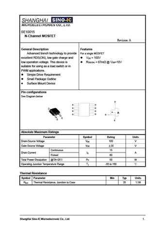
SE10015 N-Channel MOSFET Revision A General Description Features For a single MOSFET Advanced trench technology to provide excellent RDS(ON), low gate charge and V =100V DS low operation voltage. This device is R =67m @V =10V DS(ON) GS suitable for using as a load switch or in PWM applications. Simple Drive Requirement Small Package Outline Surface Mount De... See More ⇒
9.6. Size:289K cn sino-ic
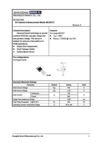
se100130ga.pdf
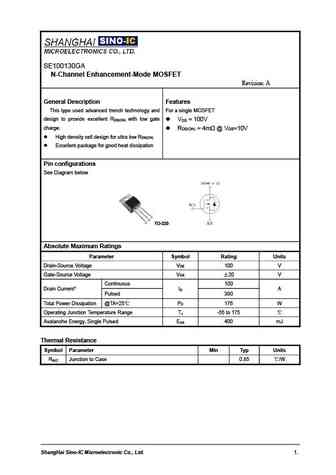
SE100130GA N-Channel Enhancement-Mode MOSFET Revision A General Description Features This type used advanced trench technology and For a single MOSFET design to provide excellent R with low gate DS(ON) V =100V DS charge. R =4m @V =10V DS(ON) GS High density cell design for ultra low R DS(ON) Excellent package for good heat dissipation Pin configurations See Di... See More ⇒
9.7. Size:576K cn sino-ic
se1003.pdf
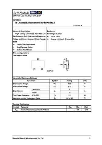
SE1003 N-Channel Enhancement-Mode MOSFET Revision A General Description Features Thigh Density Cell Design For Ultra Low For a single MOSFET On-Resistance Fully Characterized Avalanche V = 100V DS Voltage and Current Improved Shoot-Through R = 230m @ V =10V DS(ON) GS FOM Simple Drive Requirement Small Package Outline Surface Mount Device Pin configurations ... See More ⇒
9.8. Size:418K cn sino-ic
se100130a.pdf
SE100130A N-Channel Enhancement-Mode MOSFET Revision A General Description Features For a single MOSFET Advanced trench technology to provide excellent RDS(ON), low gate charge and V = 100V DS low operation voltage. This device is R =3.0m @V =10V DS(ON) GS suitable for using as a load switch or in PWM applications. Simple Drive Requirement Small Package Outline ... See More ⇒
9.9. Size:290K cn sino-ic
se100180ga.pdf
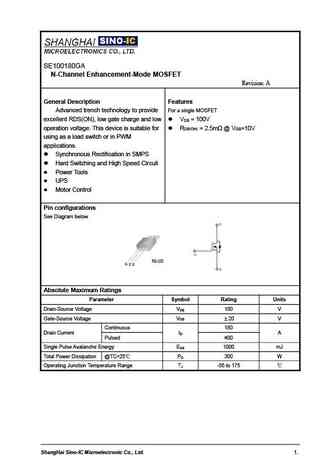
SE100180GA N-Channel Enhancement-Mode MOSFET Revision A General Description Features For a single MOSFET Advanced trench technology to provide excellent RDS(ON), low gate charge and low V =100V DS operation voltage. This device is suitable for R =2.5m @V =10V DS(ON) GS using as a load switch or in PWM applications. Synchronous Rectification in SMPS Hard Switchin... See More ⇒
9.10. Size:420K cn sino-ic
se10030a.pdf
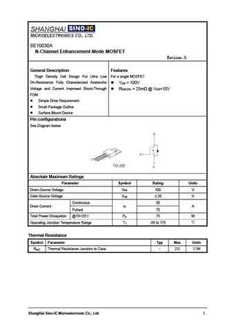
SE10030A N-Channel Enhancement-Mode MOSFET Revision A General Description Features Thigh Density Cell Design For Ultra Low For a single MOSFET On-Resistance Fully Characterized Avalanche V =100V DS Voltage and Current Improved Shoot-Through R =25m @V =10V DS(ON) GS FOM Simple Drive Requirement Small Package Outline Surface Mount Device Pin configurations ... See More ⇒
Otros transistores... SDT9304
, SDT9305
, SDT9306
, SDT9307
, SDT9308
, SDT9309
, SE0566
, SE1001
, TIP35C
, SE1022
, SE1730
, SE2001
, SE2002
, SE3001
, SE3002
, SE3005
, SE4001
.