ST10 Equivalente. Reemplazo. Hoja de especificaciones. Principales características
Número de Parte: ST10
Material: Si
Polaridad de transistor: NPN
ESPECIFICACIONES MÁXIMAS
Disipación total del dispositivo (Pc): 0.2 W
Tensión colector-base (Vcb): 15 V
Tensión colector-emisor (Vce): 15 V
Tensión emisor-base (Veb): 2 V
Corriente del colector DC máxima (Ic): 0.025 A
Temperatura operativa máxima (Tj): 200 °C
CARACTERÍSTICAS ELÉCTRICAS
Transición de frecuencia (fT): 15 MHz
Capacitancia de salida (Cc): 5 pF
Ganancia de corriente contínua (hFE): 17
Encapsulados: TO5
Búsqueda de reemplazo de ST10
- Selecciónⓘ de transistores por parámetros
ST10 datasheet
bst100.pdf
DISCRETE SEMICONDUCTORS DATA SHEET BST100 P-channel enhancement mode vertical D-MOS transistor April 1995 Product specification File under Discrete Semiconductors, SC13b Philips Semiconductors Product specification P-channel enhancement mode vertical BST100 D-MOS transistor DESCRIPTION QUICK REFERENCE DATA P-channel vertical D-MOS transistor Drain-source voltage -VDS max. 60 V T
kst10.pdf
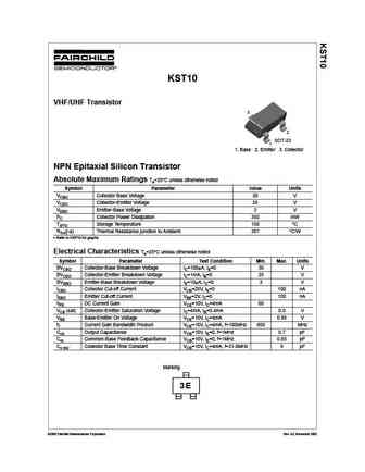
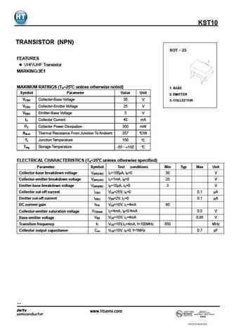
KST10 VHF/UHF Transistor 3 2 SOT-23 1 1. Base 2. Emitter 3. Collector NPN Epitaxial Silicon Transistor Absolute Maximum Ratings Ta=25 C unless otherwise noted Symbol Parameter Value Units VCBO Collector Base Voltage 30 V VCEO Collector-Emitter Voltage 25 V VEBO Emitter-Base Voltage 3 V PC Collector Power Dissipation 350 mW TSTG Storage Temperature 150 C RTH(j-a) Thermal Resis
sst108 sst109 sst110.pdf
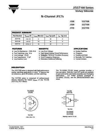
N-Channel JFET Switch LLC J108 J110 / SST108 SST110 FEATURES APPLICATIONS Low Cost Analog Switches Automated Insertion Package Choppers Low Insertion Loss Commutators No Offset or Error Voltages Generated by Closed Switch Low-Noise Audio Amplifiers Purely Resistive ABSOLUTE MAXIMUM RATINGS High Isolation
Otros transistores... SS9011 , SS9012 , SS9013 , SS9014 , SS9015 , SS9016 , SS9018 , ST03 , BC547 , ST1026 , ST1050 , ST11 , ST12 , ST1290 , ST13 , ST14 , ST150 .
History: CTP1400
History: CTP1400
🌐 : EN ES РУ

Liste
Recientemente añadidas las descripciónes de los transistores:
BJT: GA1A4M | SBT42 | 2SA200-Y | 2SA200-O | 2SD882-Q | 2SD882-P | 2SD882-E | 2SC945-L | 2SC945-H | 2SC4226-R23 | 2SC3357-F | 2SC3357-E | 2SC3356-R26 | 2SC3356-R24 | 2SC3356-R23 | 2SB772-Q | 2SB772-P | 2SB772-E | 2SA1015-L | 2SA1015-H | HSS8550
Popular searches
ksc1845 | c1815 transistor | 2sc1815 | irfz44 | 2n5551 | irf540n | irf3205 mosfet | 2n3055