ST10 Specs and Replacement
Type Designator: ST10
Material of Transistor: Si
Polarity: NPN
Absolute Maximum Ratings
Maximum Collector Power Dissipation (Pc): 0.2 W
Maximum Collector-Base Voltage |Vcb|: 15 V
Maximum Collector-Emitter Voltage |Vce|: 15 V
Maximum Emitter-Base Voltage |Veb|: 2 V
Maximum Collector Current |Ic max|: 0.025 A
Max. Operating Junction Temperature (Tj): 200 °C
Electrical Characteristics
Transition Frequency (ft): 15 MHz
Collector Capacitance (Cc): 5 pF
Forward Current Transfer Ratio (hFE), MIN: 17
Noise Figure, dB: -
Package: TO5
- BJT ⓘ Cross-Reference Search
ST10 datasheet
0.1. Size:67K philips
bst100.pdf 
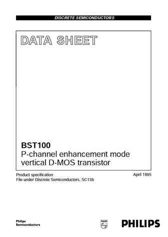
DISCRETE SEMICONDUCTORS DATA SHEET BST100 P-channel enhancement mode vertical D-MOS transistor April 1995 Product specification File under Discrete Semiconductors, SC13b Philips Semiconductors Product specification P-channel enhancement mode vertical BST100 D-MOS transistor DESCRIPTION QUICK REFERENCE DATA P-channel vertical D-MOS transistor Drain-source voltage -VDS max. 60 V T... See More ⇒
0.2. Size:44K fairchild semi
kst10.pdf
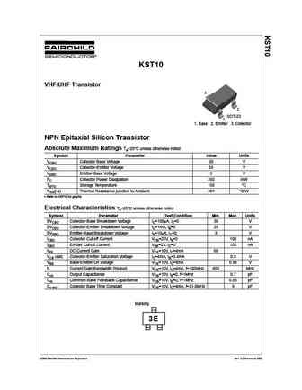
KST10 VHF/UHF Transistor 3 2 SOT-23 1 1. Base 2. Emitter 3. Collector NPN Epitaxial Silicon Transistor Absolute Maximum Ratings Ta=25 C unless otherwise noted Symbol Parameter Value Units VCBO Collector Base Voltage 30 V VCEO Collector-Emitter Voltage 25 V VEBO Emitter-Base Voltage 3 V PC Collector Power Dissipation 350 mW TSTG Storage Temperature 150 C RTH(j-a) Thermal Resis... See More ⇒
0.4. Size:21K calogic
sst108 sst109 sst110.pdf
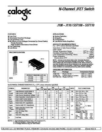
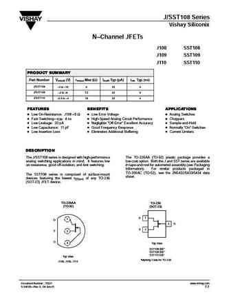
N-Channel JFET Switch LLC J108 J110 / SST108 SST110 FEATURES APPLICATIONS Low Cost Analog Switches Automated Insertion Package Choppers Low Insertion Loss Commutators No Offset or Error Voltages Generated by Closed Switch Low-Noise Audio Amplifiers Purely Resistive ABSOLUTE MAXIMUM RATINGS High Isolation... See More ⇒
0.5. Size:386K htsemi
kst10.pdf
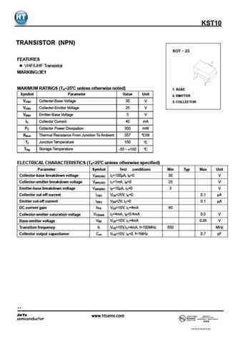
KST10 TRANSISTOR (NPN) SOT 23 FEATURES VHF/UHF Transistor MARKING 3E1 MAXIMUM RATINGS (Ta=25 unless otherwise noted) 1. BASE Symbol Parameter Value Unit 2. EMITTER V Collector-Base Voltage 30 V CBO 3. COLLECTOR V Collector-Emitter Voltage 25 V CEO V Emitter-Base Voltage 3 V EBO I Collector Current 40 mA C PC Collector Power Dissipation 350 mW R Therma... See More ⇒
0.6. Size:1277K stansontech
st1004srg.pdf
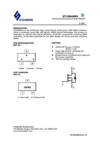
ST1004SRG N Channel Enhancement Mode MOSFET 2.0A DESCRIPTION ST1004SRG is the N-Channel logic enhancement mode power field effect transistor which is produced using high cell density, DMOS trench technology. The process is especially to improve the overall efficiency of DC/DC conventional switching PWM controllers. It has been optimized for low gate charge, low R and fast switchi... See More ⇒
0.7. Size:657K stansontech
st1005srg.pdf
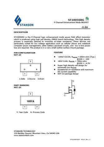
ST1005SRG P Channel Enhancement Mode MOSFET -0.8A DESCRIPTION ST1005SRG is the P-Channel logic enhancement mode power field effect transistor which is produced using high cell density, DMOS trench technology. This high density process is especially tailored to minimize on-state resistance. These devices are particularly suited for low voltage application such as cellular phone an... See More ⇒
0.8. Size:1738K stansontech
st10e4.pdf
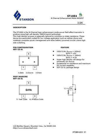
ST10E4 N Channel Enhancement Mode MOSFET 3.0A DESCRIPTION The ST10E4 is the N-Channel logic enhancement mode power field effect transistor is produce using high cell density, DMOS trench technology. This high-density process is especially tailored to minimize on-state resistance. These device are particularly suited for low voltage application such as cellular phone and notebo... See More ⇒
0.9. Size:716K stansontech
st1002.pdf
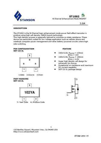
ST1002 N Channel Enhancement Mode MOSFET 3.0A DESCRIPTION The ST1002 is the N-Channel logic enhancement mode power field effect transistor is produce using high cell density, DMOS trench technology. This high-density process is especially tailored to minimize on-state resistance. These device are particularly suited for low voltage application such as cellular phone and notebo... See More ⇒
0.10. Size:1070K jestek
jst100n30t2.pdf
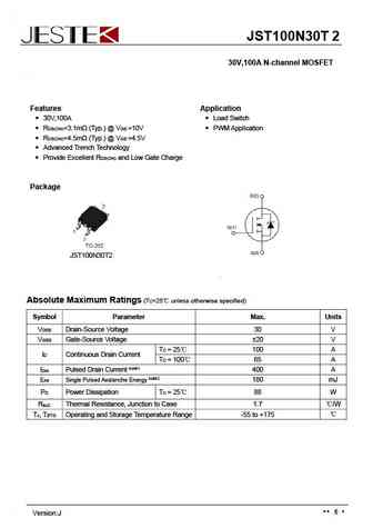
JST100N30T2 30V,100A N-channel MOSFET Features Application 30V,100A Load Switch R =3.1m (Typ.) @ V =10V PWM Application DS(ON) GS R =4.5m (Typ.) @ V =4.5V DS(ON) GS Advanced Trench Technology Provide Excellent R and Low Gate Charge DS(ON) Package JST100N30T2 Absolute Maximum Ratings (T =25 unless otherwise specified) C Symbol Parameter ... See More ⇒
Detailed specifications: SS9011, SS9012, SS9013, SS9014, SS9015, SS9016, SS9018, ST03, BC547, ST1026, ST1050, ST11, ST12, ST1290, ST13, ST14, ST150
Keywords - ST10 pdf specs
ST10 cross reference
ST10 equivalent finder
ST10 pdf lookup
ST10 substitution
ST10 replacement