TK20 Datasheet. Equivalente. Reemplazo. Hoja de especificaciones. Principales características
Número de Parte: TK20 📄📄
Material: Ge
Polaridad de transistor: PNP
ESPECIFICACIONES MÁXIMAS
Disipación total del dispositivo (Pc): 0.2 W
Tensión colector-base (Vcb): 30 V
Tensión colector-emisor (Vce): 12 V
Tensión emisor-base (Veb): 30 V
Corriente del colector DC máxima (Ic): 0.05 A
Temperatura operativa máxima (Tj): 75 °C
CARACTERÍSTICAS ELÉCTRICAS
Transición de frecuencia (fT): 3 MHz
Ganancia de corriente contínua (hFE): 20
Encapsulados: X18
📄📄 Copiar
Búsqueda de reemplazo de TK20
- Selecciónⓘ de transistores por parámetros
TK20 datasheet
0.1. Size:917K st
stk20n75f3.pdf 
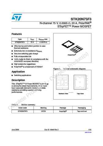
STK20N75F3 N-channel 75 V, 0.0065 , 20 A, PolarPAK STripFET Power MOSFET Features VDSS RDS(on) max Type STK20N75F3 75 V
0.2. Size:236K toshiba
tk20s06k3l.pdf

TK20S06K3L MOSFETs Silicon N-channel MOS (U-MOS ) TK20S06K3L TK20S06K3L TK20S06K3L TK20S06K3L 1. Applications 1. Applications 1. Applications 1. Applications Motor Drivers DC-DC Converters Switching Voltage Regulators 2. Features 2. Features 2. Features 2. Features (1) Low drain-source on-resistance RDS(ON) = 23 m (typ.) (VGS = 10 V) (2) Low leakage current
0.3. Size:245K toshiba
tk20n60w.pdf
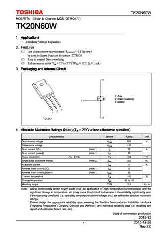
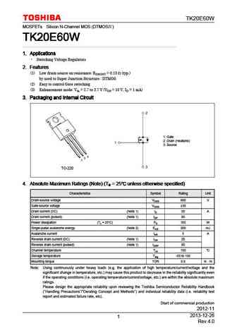
TK20N60W MOSFETs Silicon N-Channel MOS (DTMOS ) TK20N60W TK20N60W TK20N60W TK20N60W 1. Applications 1. Applications 1. Applications 1. Applications Switching Voltage Regulators 2. Features 2. Features 2. Features 2. Features (1) Low drain-source on-resistance RDS(ON) = 0.13 (typ.) by used to Super Junction Structure DTMOS (2) Easy to control Gate switching (3) En
0.4. Size:239K toshiba
tk20n60w5.pdf
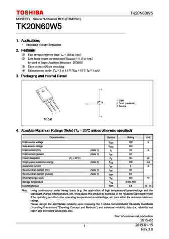
TK20N60W5 MOSFETs Silicon N-Channel MOS (DTMOS ) TK20N60W5 TK20N60W5 TK20N60W5 TK20N60W5 1. Applications 1. Applications 1. Applications 1. Applications Switching Voltage Regulators 2. Features 2. Features 2. Features 2. Features (1) Fast reverse recovery time trr = 110 ns (typ.) (2) Low drain-source on-resistance RDS(ON) = 0.15 (typ.) by used to Super Junction Str
0.5. Size:273K toshiba
tk200f04n1l.pdf
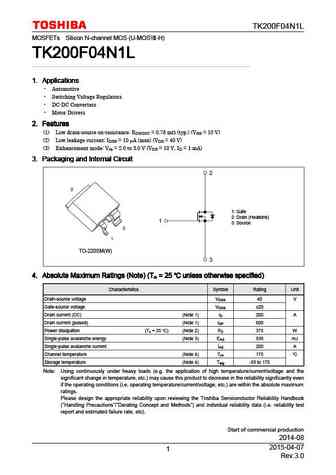
TK200F04N1L MOSFETs Silicon N-channel MOS (U-MOS -H) TK200F04N1L TK200F04N1L TK200F04N1L TK200F04N1L 1. Applications 1. Applications 1. Applications 1. Applications Automotive Switching Voltage Regulators DC-DC Converters Motor Drivers 2. Features 2. Features 2. Features 2. Features (1) Low drain-source on-resistance RDS(ON) = 0.78 m (typ.) (VGS = 10 V)
0.6. Size:271K toshiba
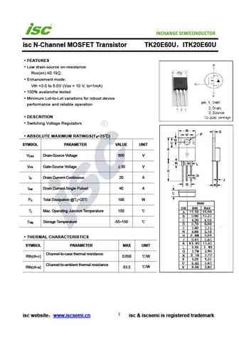
tk20e60u.pdf
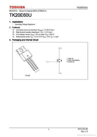
TK20E60U MOSFETs Silicon N-Channel MOS (DTMOS ) TK20E60U TK20E60U TK20E60U TK20E60U 1. Applications 1. Applications 1. Applications 1. Applications Switching Voltage Regulators 2. Features 2. Features 2. Features 2. Features (1) Low drain-source on-resistance RDS(ON) = 0.165 (typ.) (2) High forward transfer admittance Yfs = 12 S (typ.) (3) Low leakage current IDS
0.7. Size:234K toshiba
tk20a60w5.pdf
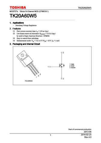
TK20A60W5 MOSFETs Silicon N-Channel MOS (DTMOS ) TK20A60W5 TK20A60W5 TK20A60W5 TK20A60W5 1. Applications 1. Applications 1. Applications 1. Applications Switching Voltage Regulators 2. Features 2. Features 2. Features 2. Features (1) Fast reverse recovery time trr = 110 ns (typ.) (2) Low drain-source on-resistance RDS(ON) = 0.15 (typ.) by used to Super Junction Str
0.8. Size:242K toshiba
tk20g60w.pdf
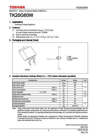
TK20G60W MOSFETs Silicon N-Channel MOS (DTMOS ) TK20G60W TK20G60W TK20G60W TK20G60W 1. Applications 1. Applications 1. Applications 1. Applications Switching Voltage Regulators 2. Features 2. Features 2. Features 2. Features (1) Low drain-source on-resistance RDS(ON) = 0.13 (typ.) by used to Super Junction Structure DTMOS (2) Easy to control Gate switching (3) En
0.9. Size:232K toshiba
tk20a25d.pdf

TK20A25D MOSFETs Silicon N-Channel MOS ( -MOS ) TK20A25D TK20A25D TK20A25D TK20A25D 1. Applications 1. Applications 1. Applications 1. Applications Switching Voltage Regulators 2. Features 2. Features 2. Features 2. Features (1) Low drain-source on-resistance RDS(ON) = 0.073 (typ.) (2) Low leakage current IDSS = 10 A (max) (VDS = 250 V) (3) Enhancement mode Vth
0.10. Size:236K toshiba
tk20s04k3l.pdf
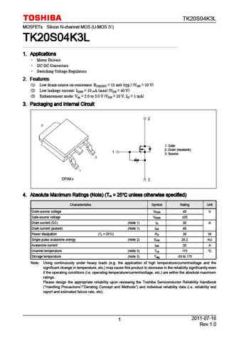
TK20S04K3L MOSFETs Silicon N-channel MOS (U-MOS ) TK20S04K3L TK20S04K3L TK20S04K3L TK20S04K3L 1. Applications 1. Applications 1. Applications 1. Applications Motor Drivers DC-DC Converters Switching Voltage Regulators 2. Features 2. Features 2. Features 2. Features (1) Low drain-source on-resistance RDS(ON) = 11 m (typ.) (VGS = 10 V) (2) Low leakage current
0.11. Size:191K toshiba
tk20x60u.pdf
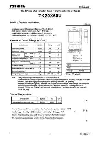
TK20X60U TOSHIBA Field Effect Transistor Silicon N Channel MOS Type (DTMOS ) TK20X60U Switching Regulator Applications Unit mm Low drain-source ON resistance RDS (ON) = 0.175 (typ.) High forward transfer admittance Yfs = 12 S (typ.) Low leakage current IDSS = 100 A (max) (VDS = 600 V) Enhancement-mode Vth = 3.0 to 5.0 V (VDS = 10 V, ID = 1 mA)
0.12. Size:237K toshiba
tk20p04m1.pdf
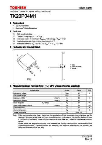
TK20P04M1 MOSFETs Silicon N-Channel MOS (U-MOS -H) TK20P04M1 TK20P04M1 TK20P04M1 TK20P04M1 1. Applications 1. Applications 1. Applications 1. Applications DC-DC Converters Switching Voltage Regulators 2. Features 2. Features 2. Features 2. Features (1) High-speed switching (2) Low gate charge QSW = 3.7 nC (typ.) (3) Low drain-source on-resistance RDS(ON) = 19 m
0.13. Size:228K toshiba
tk20h50c.pdf
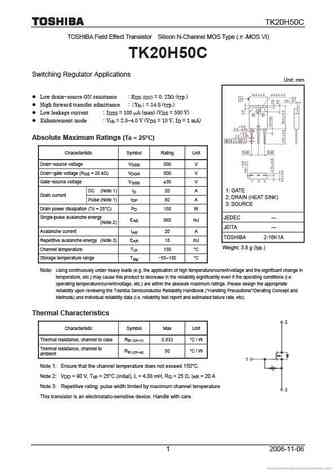
TK20H50C TOSHIBA Field Effect Transistor Silicon N-Channel MOS Type ( -MOS VI) TK20H50C Switching Regulator Applications Unit mm Low drain-source ON resistance RDS (ON) = 0. 23 (typ.) High forward transfer admittance Yfs = 14 S (typ.) Low leakage current IDSS = 100 A (max) (VDS = 500 V) Enhancement mode Vth = 2.0 4.0 V (VDS = 10 V, ID = 1 mA) Absolute M
0.14. Size:239K toshiba
tk20j60w5.pdf
TK20J60W5 MOSFETs Silicon N-Channel MOS (DTMOS ) TK20J60W5 TK20J60W5 TK20J60W5 TK20J60W5 1. Applications 1. Applications 1. Applications 1. Applications Switching Voltage Regulators 2. Features 2. Features 2. Features 2. Features (1) Fast reverse recovery time trr = 110 ns (typ.) (2) Low drain-source on-resistance RDS(ON) = 0.15 (typ.) by used to Super Junction Str
0.15. Size:273K toshiba
tk20a60u.pdf
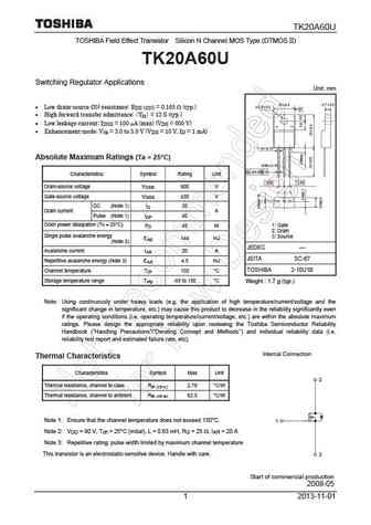
TK20A60U TOSHIBA Field Effect Transistor Silicon N Channel MOS Type (DTMOS II) TK20A60U Switching Regulator Applications Unit mm Low drain-source ON-resistance RDS (ON) = 0.165 (typ.) High forward transfer admittance Yfs = 12 S (typ.) Low leakage current IDSS = 100 A (max) (VDS = 600 V) Enhancement-mode Vth = 3.0 to 5.0 V (VDS = 10 V, ID = 1 mA)
0.16. Size:243K toshiba
tk20a60w.pdf
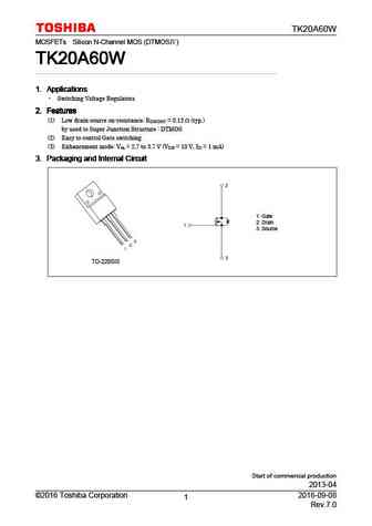
TK20A60W MOSFETs Silicon N-Channel MOS (DTMOS ) TK20A60W TK20A60W TK20A60W TK20A60W 1. Applications 1. Applications 1. Applications 1. Applications Switching Voltage Regulators 2. Features 2. Features 2. Features 2. Features (1) Low drain-source on-resistance RDS(ON) = 0.13 (typ.) by used to Super Junction Structure DTMOS (2) Easy to control Gate switching (3) En
0.17. Size:249K toshiba
tk20e60w.pdf
TK20E60W MOSFETs Silicon N-Channel MOS (DTMOS ) TK20E60W TK20E60W TK20E60W TK20E60W 1. Applications 1. Applications 1. Applications 1. Applications Switching Voltage Regulators 2. Features 2. Features 2. Features 2. Features (1) Low drain-source on-resistance RDS(ON) = 0.13 (typ.) by used to Super Junction Structure DTMOS (2) Easy to control Gate switching (3) En
0.18. Size:205K toshiba
tk20a60t.pdf
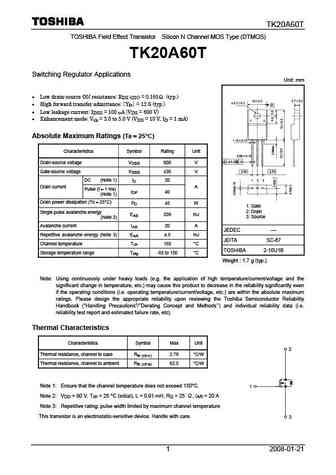
TK20A60T TOSHIBA Field Effect Transistor Silicon N Channel MOS Type (DTMOS) TK20A60T Switching Regulator Applications Unit mm Low drain-source ON resistance RDS (ON) = 0.165 (typ.) High forward transfer admittance Yfs = 12 S (typ.) Low leakage current IDSS = 100 A (VDS = 600 V) Enhancement-mode Vth = 3.0 to 5.0 V (VDS = 10 V, ID = 1 mA) Absolute M
0.19. Size:242K toshiba
tk20j60w.pdf

TK20J60W MOSFETs Silicon N-Channel MOS (DTMOS ) TK20J60W TK20J60W TK20J60W TK20J60W 1. Applications 1. Applications 1. Applications 1. Applications Switching Voltage Regulators 2. Features 2. Features 2. Features 2. Features (1) Low drain-source on-resistance RDS(ON) = 0.13 (typ.) by used to Super Junction Structure DTMOS (2) Easy to control Gate switching (3) En
0.20. Size:152K toshiba
tk20j60t.pdf
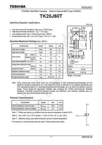
TK20J60T TOSHIBA Field Effect Transistor Silicon N Channel MOS Type (DTMOS) TK20J60T Switching Regulator Applications Unit mm 3.2 0.2 15.9max. Low drain-source ON resistance RDS (ON) = 0.165 (typ.) High forward transfer admittance Yfs = 12 S (typ.) Low leakage current IDSS = 100 A (max) (VDS = 600 V) Enhancement-mode Vth = 3.0 to 5.0 V (VD
0.21. Size:196K toshiba
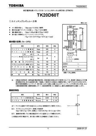
tk20d60u.pdf
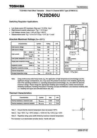
TK20D60U TOSHIBA Field Effect Transistor Silicon N Channel MOS Type (DTMOS ) TK20D60U Switching Regulator Applications Unit mm 10.0 0.3 A 9.5 0.2 0.6 0.1 Low drain-source ON-resistance RDS (ON) = 0.165 (typ.) 3.65 0.2 High forward transfer admittance Yfs = 12 S (typ.) Low leakage current IDSS = 100 A (VDS = 600 V) Enhancement
0.23. Size:239K toshiba
tk20v60w.pdf
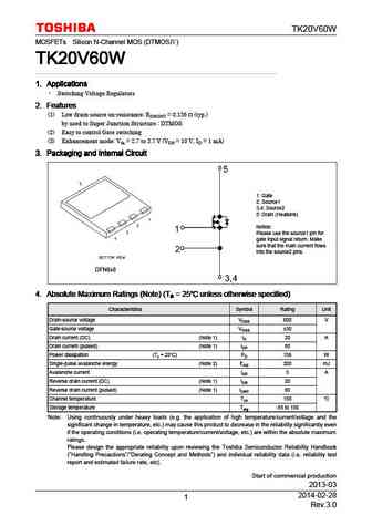
TK20V60W MOSFETs Silicon N-Channel MOS (DTMOS ) TK20V60W TK20V60W TK20V60W TK20V60W 1. Applications 1. Applications 1. Applications 1. Applications Switching Voltage Regulators 2. Features 2. Features 2. Features 2. Features (1) Low drain-source on-resistance RDS(ON) = 0.136 (typ.) by used to Super Junction Structure DTMOS (2) Easy to control Gate switching (3) E
0.24. Size:241K toshiba
tk20c60w.pdf

TK20C60W MOSFETs Silicon N-Channel MOS (DTMOS ) TK20C60W TK20C60W TK20C60W TK20C60W 1. Applications 1. Applications 1. Applications 1. Applications Switching Voltage Regulators 2. Features 2. Features 2. Features 2. Features (1) Low drain-source on-resistance RDS(ON) = 0.13 (typ.) by used to Super Junction Structure DTMOS (2) Easy to control Gate switching (3) En
0.25. Size:193K toshiba
tk20j50d.pdf
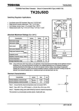
TK20J50D TOSHIBA Field Effect Transistor Silicon N Channel MOS Type ( -MOS VII) TK20J50D Switching Regulator Applications Unit mm 15.9 MAX. 3.2 0.2 Low drain-source ON-resistance RDS (ON) = 0.22 (typ.) High forward transfer admittance Yfs = 8.5 S (typ.) Low leakage current IDSS = 10 A (max) (VDS = 500 V) Enhancement mode Vth = 2.0 to 4.0 V (V
0.26. Size:192K toshiba
tk20j60u.pdf
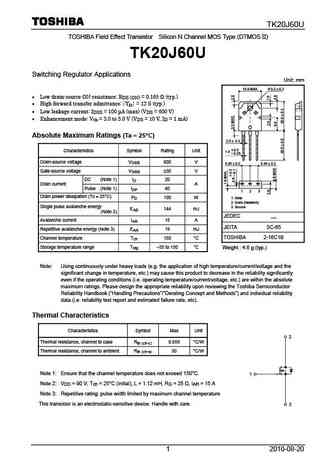
TK20J60U TOSHIBA Field Effect Transistor Silicon N Channel MOS Type (DTMOS II) TK20J60U Switching Regulator Applications Unit mm 15.9 MAX. 3.2 0.2 Low drain-source ON-resistance RDS (ON) = 0.165 (typ.) High forward transfer admittance Yfs = 12 S (typ.) Low leakage current IDSS = 100 A (max) (VDS = 600 V) Enhancement mode Vth = 3.0 to 5.0 V
0.27. Size:219K toshiba
tk20a20d.pdf
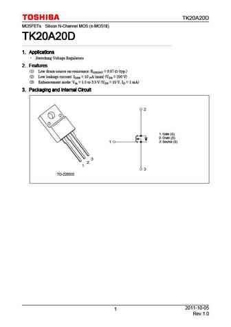
TK20A20D MOSFETs Silicon N-Channel MOS ( -MOS ) TK20A20D TK20A20D TK20A20D TK20A20D 1. Applications 1. Applications 1. Applications 1. Applications Switching Voltage Regulators 2. Features 2. Features 2. Features 2. Features (1) Low drain-source on-resistance RDS(ON) = 0.07 (typ.) (2) Low leakage current IDSS = 10 A (max) (VDS = 200 V) (3) Enhancement mode Vth =
0.28. Size:243K toshiba
tk20e60w5.pdf
TK20E60W5 MOSFETs Silicon N-Channel MOS (DTMOS ) TK20E60W5 TK20E60W5 TK20E60W5 TK20E60W5 1. Applications 1. Applications 1. Applications 1. Applications Switching Voltage Regulators 2. Features 2. Features 2. Features 2. Features (1) Fast reverse recovery time trr = 110 ns (typ.) (2) Low drain-source on-resistance RDS(ON) = 0.15 (typ.) by used to Super Junction Str
0.29. Size:270K toshiba
tk20v60w5.pdf
TK20V60W5 MOSFETs Silicon N-Channel MOS (DTMOS ) TK20V60W5 TK20V60W5 TK20V60W5 TK20V60W5 1. Applications 1. Applications 1. Applications 1. Applications Switching Voltage Regulators 2. Features 2. Features 2. Features 2. Features (1) Fast reverse recovery time trr = 110 ns (typ.) (2) Low drain-source on-resistance RDS(ON) = 0.156 (typ.) (3) Easy to control Gate switc
0.30. Size:162K ixys
ixtk200n10p.pdf
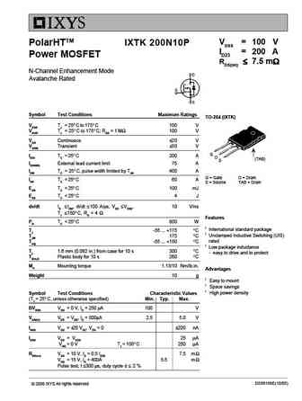
VDSS = 100 V IXTK 200N10P PolarHTTM ID25 = 200 A Power MOSFET RDS(on) 7.5 m N-Channel Enhancement Mode Avalanche Rated Symbol Test Conditions Maximum Ratings TO-264 (IXTK) VDSS TJ = 25 C to 175 C 100 V VDGR TJ = 25 C to 175 C; RGS = 1 M 100 V VGS Continuous 20 V VGSM Transient 30 V G ID25 TC = 25 C 200 A D (TAB) S ID
0.31. Size:129K ixys
ixtk20n150 ixtx20n150.pdf
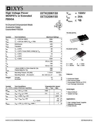
High Voltage Power VDSS = 1500V IXTK20N150 MOSFETs w/ Extended ID25 = 20A IXTX20N150 FBSOA RDS(on)
0.32. Size:530K first silicon
ftk2012.pdf
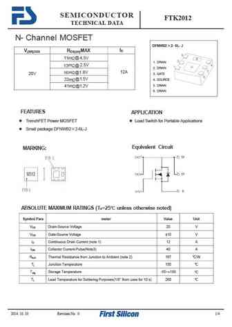
SEMICONDUCTOR FTK2012 TECHNICAL DATA N-Channel MOSFET DFNWB2 2-6L-J ID V(BR)DSS RDS(on)MAX m @ 4.5V 11 1. DRAIN @ 13m 2.5V 2. DRAIN A m @1.8V 12 16 20V 3. GATE 4. SOURCE 22m @1.5V 5. DRAIN 41m @1.2V 6. DRAIN FEATURES APPLICATION TrenchFET Power MOSFET Load Switch for Portable Applications Small package DFNWB2 2-6L-J Equivalent Circui
0.33. Size:425K first silicon
ftk20n06d.pdf
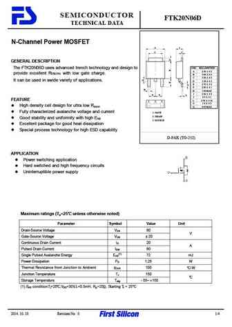
SEMICONDUCTOR FTK20N06D TECHNICAL DATA N-Channel Power MOSFET A I C J GENERAL DESCRIPTION The FTK20N06D uses advanced trench technology and design to DIM MILLIMETERS A 6 50 0 2 provide excellent RDS(ON) with low gate charge. B 5 60 0 2 C 5 20 0 2 It can be used in awide variety of applications. D 1 50 0 2 E 2 70 0 2 F 2 30 0 1 H H 1 00 MAX I 2 30 0
0.34. Size:818K first silicon
ftk2005dfn23.pdf
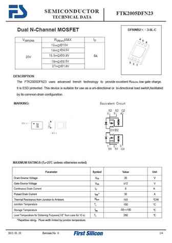
SEMICONDUCTOR FTK2005DFN23 TECHNICAL DATA DFNWB2 3-6L-C Dual N-Channel MOSFET ID V(BR)DSS RDS(on)MAX 13 V m @10 14 @4.5V m 15.5m @3.8V 8 A 20V .5V 19m @2 27m @1.8V DESCRIPTION The FTK2005DFN23 uses advanced trench technology to provide excellent RDS(ON) low gate charge. It is ESD protected. This device is suitable for use as a uni-directional or bi-direction
0.35. Size:883K jiejie micro
jmtk2007a.pdf
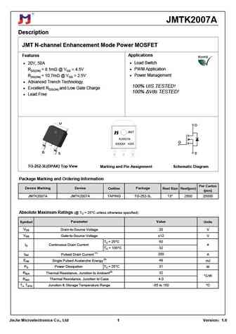
JMTK2007A Description JMT N-channel Enhancement Mode Power MOSFET Features Applications 20V, 50A Load Switch RDS(ON)
0.36. Size:1119K jiejie micro
jmtk2006a.pdf
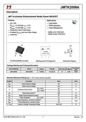
JMTK2006A Description JMT N-channel Enhancement Mode Power MOSFET Features Applications 20V, 60A Load Switch RDS(ON)
0.37. Size:769K cn vbsemi
tk20s06k3l.pdf
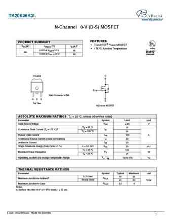
TK20S06K3L www.VBsemi.tw N-Channel 6 0-V (D-S) MOSFET FEATURES PRODUCT SUMMARY TrenchFET Power MOSFET VDS (V) rDS(on) ( ) ID (A)a Available 175 C Junction Temperature 0.025 at VGS = 10 V 35 RoHS* 60 0.030 at VGS = 4.5 V 30 COMPLIANT TO-252 D G Drain Connected to Tab G D S S Top View N-Channel MOSFET ABSOLUTE MAXIMUM RATINGS TC = 25 C, unless otherwise
0.39. Size:253K inchange semiconductor
tk20a60w5.pdf
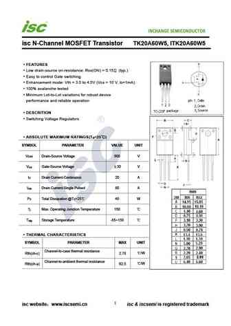
INCHANGE Semiconductor isc N-Channel MOSFET Transistor TK20A60W5, ITK20A60W5 FEATURES Low drain-source on-resistance RDS(ON) = 0.15 (typ.) Easy to control Gate switching Enhancement mode Vth = 3.0 to 4.5V (VDS = 10 V, ID=1mA) 100% avalanche tested Minimum Lot-to-Lot variations for robust device performance and reliable operation DESCRITION Switching Voltage Regula
0.40. Size:251K inchange semiconductor
tk20a25d.pdf
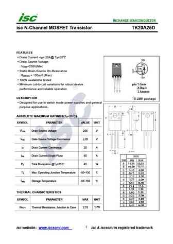
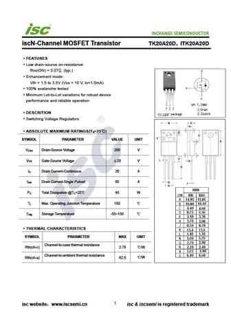
isc N-Channel MOSFET Transistor TK20A25D FEATURES Drain Current I = 20A@ T =25 D C Drain Source Voltage- V =250V(Min) DSS Static Drain-Source On-Resistance R = 100m (Max) DS(on) 100% avalanche tested Minimum Lot-to-Lot variations for robust device performance and reliable operation DESCRIPTION Designed for use in switch mode power supplies and general purpo
0.41. Size:253K inchange semiconductor
tk20a60u.pdf
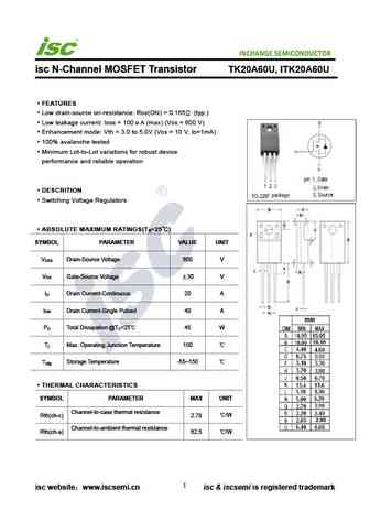
INCHANGE Semiconductor isc N-Channel MOSFET Transistor TK20A60U, ITK20A60U FEATURES Low drain-source on-resistance RDS(ON) = 0.165 (typ.) Low leakage current IDSS = 100 A (max) (VDS = 600 V) Enhancement mode Vth = 3.0 to 5.0V (VDS = 10 V, ID=1mA) 100% avalanche tested Minimum Lot-to-Lot variations for robust device performance and reliable operation DESCRITION S
0.42. Size:253K inchange semiconductor
tk20a60w.pdf
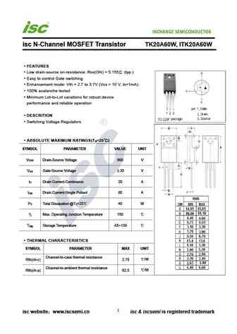
INCHANGE Semiconductor isc N-Channel MOSFET Transistor TK20A60W, ITK20A60W FEATURES Low drain-source on-resistance RDS(ON) = 0.155 (typ.) Easy to control Gate switching Enhancement mode Vth = 2.7 to 3.7V (VDS = 10 V, ID=1mA) 100% avalanche tested Minimum Lot-to-Lot variations for robust device performance and reliable operation DESCRITION Switching Voltage Regulat
0.43. Size:220K inchange semiconductor
tk20j50d.pdf
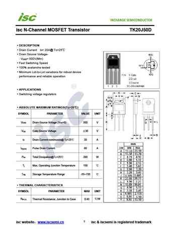
isc N-Channel MOSFET Transistor TK20J50D DESCRIPTION Drain Current I = 20A@ T =25 D C Drain Source Voltage- V = 500V(Min) DSS Fast Switching Speed 100% avalanche tested Minimum Lot-to-Lot variations for robust device performance and reliable operation APPLICATIONS Switching voltage regulators ABSOLUTE MAXIMUM RATINGS(T =25 ) C SYMBOL PARAMETER VALUE UNIT
0.44. Size:253K inchange semiconductor
tk20a20d.pdf
INCHANGE Semiconductor iscN-Channel MOSFET Transistor TK20A20D ITK20A20D FEATURES Low drain-source on-resistance RDS(ON) = 0.07 (typ.) Enhancement mode Vth = 1.5 to 3.5V (VDS = 10 V, ID=1.0mA) 100% avalanche tested Minimum Lot-to-Lot variations for robust device performance and reliable operation DESCRITION Switching Voltage Regulators ABSOLUTE MAXIMUM RATINGS
Otros transistores... TIX891, TIX896, TIXM107, TIXM108, TIXM13, TIXP39, TIXP40, TK100, BC547B, TK200, TK200A, TK201, TK201A, TK202A, TK203A, TK20B, TK20C