TK25 Datasheet. Equivalente. Reemplazo. Hoja de especificaciones. Principales características
Número de Parte: TK25 📄📄
Material: Ge
Polaridad de transistor: PNP
ESPECIFICACIONES MÁXIMAS
Disipación total del dispositivo (Pc): 0.2 W
Tensión colector-base (Vcb): 20 V
Tensión colector-emisor (Vce): 6 V
Tensión emisor-base (Veb): 20 V
Corriente del colector DC máxima (Ic): 0.25 A
Temperatura operativa máxima (Tj): 75 °C
CARACTERÍSTICAS ELÉCTRICAS
Transición de frecuencia (fT): 6 MHz
Ganancia de corriente contínua (hFE): 20
Encapsulados: X18
📄📄 Copiar
Búsqueda de reemplazo de TK25
- Selecciónⓘ de transistores por parámetros
TK25 datasheet
0.1. Size:219K toshiba
tk25a20d.pdf 
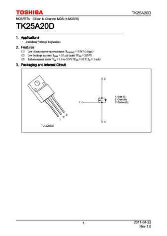
TK25A20D MOSFETs Silicon N-Channel MOS ( -MOS ) TK25A20D TK25A20D TK25A20D TK25A20D 1. Applications 1. Applications 1. Applications 1. Applications Switching Voltage Regulators 2. Features 2. Features 2. Features 2. Features (1) Low drain-source on-resistance RDS(ON) = 0.047 (typ.) (2) Low leakage current IDSS = 10 A (max) (VDS = 200 V) (3) Enhancement mode Vth
0.2. Size:236K toshiba
tk25a60x.pdf

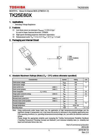
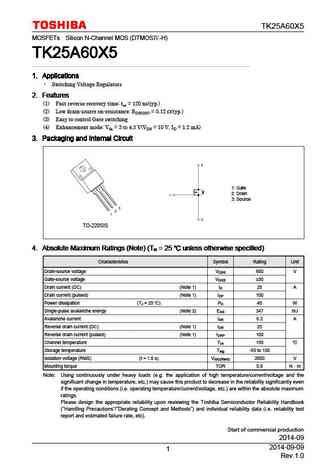
TK25A60X MOSFETs Silicon N-Channel MOS (DTMOS -H) TK25A60X TK25A60X TK25A60X TK25A60X 1. Applications 1. Applications 1. Applications 1. Applications Switching Voltage Regulators 2. Features 2. Features 2. Features 2. Features (1) Low drain-source on-resistance RDS(ON) = 0.105 (typ.) by used to Super Junction Structure DTMOS (2) High-speed switching properties wit
0.3. Size:247K toshiba
tk25e60x.pdf
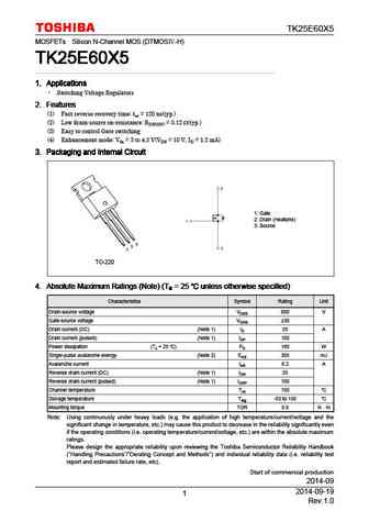
TK25E60X MOSFETs Silicon N-Channel MOS (DTMOS -H) TK25E60X TK25E60X TK25E60X TK25E60X 1. Applications 1. Applications 1. Applications 1. Applications Switching Voltage Regulators 2. Features 2. Features 2. Features 2. Features (1) Low drain-source on-resistance RDS(ON) = 0.105 (typ.) by used to Super Junction Structure DTMOS (2) High-speed switching properties wit
0.4. Size:370K toshiba
tk25n60x5.pdf

TK25N60X5 MOSFETs Silicon N-Channel MOS (DTMOS -H) TK25N60X5 TK25N60X5 TK25N60X5 TK25N60X5 1. Applications 1. Applications 1. Applications 1. Applications Switching Voltage Regulators 2. Features 2. Features 2. Features 2. Features (1) Fast reverse recovery time trr = 120 ns(typ.) (2) Low drain-source on-resistance RDS(ON) = 0.12 (typ.) (3) Easy to control Gate switc
0.5. Size:305K toshiba
tk25a10k3.pdf
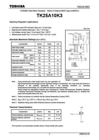
TK25A10K3 TOSHIBA Field Effect Transistor Silicon N Channel MOS Type (U-MOSIV) TK25A10K3 Swiching Regulator Applications Low drain-source ON resistance RDS (ON) = 31 m (typ.) Unit mm High forward transfer admittance Yfs = 50 S (typ.) Low leakage current IDSS = 10 A (max) (VDS = 100 V) Enhancement-model Vth = 2.0 to 4.0 V (VDS = 10 V, ID = 1 mA) Absolu
0.6. Size:238K toshiba
tk25v60x.pdf

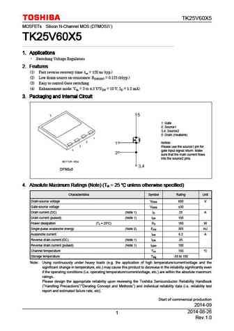
TK25V60X MOSFETs Silicon N-Channel MOS (DTMOS -H) TK25V60X TK25V60X TK25V60X TK25V60X 1. Applications 1. Applications 1. Applications 1. Applications Switching Voltage Regulators 2. Features 2. Features 2. Features 2. Features (1) Low drain-source on-resistance RDS(ON) = 0.11 (typ.) by used to Super Junction Structure DTMOS (2) High-speed switching properties with
0.7. Size:244K toshiba
tk25n60x.pdf

TK25N60X MOSFETs Silicon N-Channel MOS (DTMOS -H) TK25N60X TK25N60X TK25N60X TK25N60X 1. Applications 1. Applications 1. Applications 1. Applications Switching Voltage Regulators 2. Features 2. Features 2. Features 2. Features (1) Low drain-source on-resistance RDS(ON) = 0.105 (typ.) by used to Super Junction Structure DTMOS (2) High-speed switching properties wit
0.8. Size:363K toshiba
tk25a60x5.pdf
TK25A60X5 MOSFETs Silicon N-Channel MOS (DTMOS -H) TK25A60X5 TK25A60X5 TK25A60X5 TK25A60X5 1. Applications 1. Applications 1. Applications 1. Applications Switching Voltage Regulators 2. Features 2. Features 2. Features 2. Features (1) Fast reverse recovery time trr = 120 ns(typ.) (2) Low drain-source on-resistance RDS(ON) = 0.12 (typ.) (3) Easy to control Gate switc
0.9. Size:365K toshiba
tk25v60x5.pdf
TK25V60X5 MOSFETs Silicon N-Channel MOS (DTMOS ) TK25V60X5 TK25V60X5 TK25V60X5 TK25V60X5 1. Applications 1. Applications 1. Applications 1. Applications Switching Voltage Regulators 2. Features 2. Features 2. Features 2. Features (1) Fast reverse recovery time trr = 120 ns (typ.) (2) Low drain-source on-resistance RDS(ON) = 0.125 (typ.) (3) Easy to control Gate switc
0.10. Size:373K toshiba
tk25e60x5.pdf
TK25E60X5 MOSFETs Silicon N-Channel MOS (DTMOS -H) TK25E60X5 TK25E60X5 TK25E60X5 TK25E60X5 1. Applications 1. Applications 1. Applications 1. Applications Switching Voltage Regulators 2. Features 2. Features 2. Features 2. Features (1) Fast reverse recovery time trr = 120 ns(typ.) (2) Low drain-source on-resistance RDS(ON) = 0.12 (typ.) (3) Easy to control Gate switc
0.11. Size:241K toshiba
tk25s06n1l.pdf
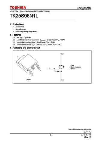
TK25S06N1L MOSFETs Silicon N-channel MOS (U-MOS -H) TK25S06N1L TK25S06N1L TK25S06N1L TK25S06N1L 1. Applications 1. Applications 1. Applications 1. Applications Automotive Motor Drivers Switching Voltage Regulators 2. Features 2. Features 2. Features 2. Features (1) AEC-Q101 qualified (2) Low drain-source on-resistance RDS(ON) = 15 m (typ.) (VGS = 10 V) (3) L
0.12. Size:560K ixys
ixtk250n10.pdf
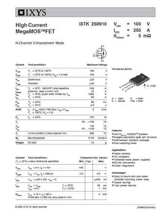
IXTK 250N10 VDSS = 100 V High Current ID25 = 250 A MegaMOSTMFET RDS(on) = 5 m N-Channel Enhancement Mode Symbol Test conditions Maximum ratings TO-264 AA (IXTK) VDSS TJ = 25 C to 150 C 100 V VDGR TJ = 25 C to 150 C; RGS = 1.0 M 100 V VGS Continuous 20 V VGSM Transient 30 V D (TAB) G ID25 TC = 25 C MOSFET chip capability 250 A D ID(RMS) Externa
0.13. Size:232K lrc
lntk2575lt1g s-lntk2575lt1g.pdf
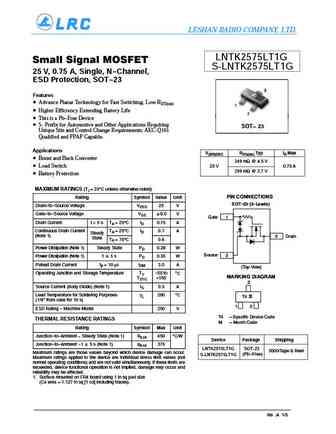
LESHAN RADIO COMPANY, LTD. LNTK2575LT1G Small Signal MOSFET S-LNTK2575LT1G 25 V, 0.75 A, Single, N-Channel, ESD Protection, SOT-23 3 Features Advance Planar Technology for Fast Switching, Low RDS(on) 1 Higher Efficiency Extending Battery Life 2 This is a Pb-Free Device S- Prefix for Automotive and Other Applications Requiring SOT 23 Unique Site and Control Ch
0.14. Size:430K first silicon
ftk25n03pdfn33.pdf
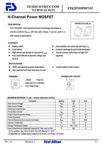
SEMICONDUCTOR FTK25N03PDFN33 TECHNICAL DATA N-Channel Power MOSFET PDFN3.3 3.3-8L-A DESCRIPTION The FTK25N03 uses advanced trench technology and design to provide excellent RDS(ON) with low gate charge. It can be used in a wide variety of applications FEATURES Battery switch Good stability and uniformity with high EAS Load switch Excellent package for good he
0.15. Size:252K inchange semiconductor
tk25a20d.pdf
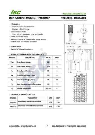
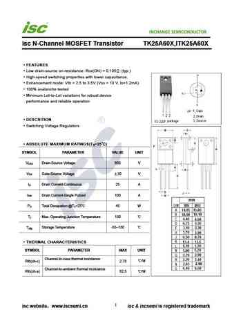
INCHANGE Semiconductor iscN-Channel MOSFET Transistor TK25A20D ITK25A20D FEATURES Low drain-source on-resistance RDS(on) = 0.047 (typ.) Enhancement mode Vth = 1.5 to 3.5V (VDS = 10 V, ID=1.0mA) 100% avalanche tested Minimum Lot-to-Lot variations for robust device performance and reliable operation DESCRITION Switching Voltage Regulators ABSOLUTE MAXIMUM RATING
0.17. Size:246K inchange semiconductor
tk25e60x.pdf
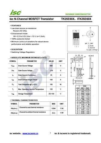
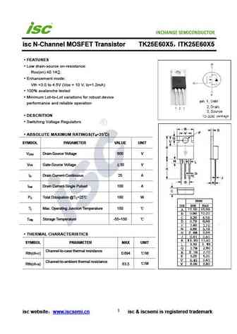
INCHANGE Semiconductor isc N-Channel MOSFET Transistor TK25E60X ITK25E60X FEATURES Low drain-source on-resistance RDS(on) 0.125 . Enhancement mode Vth =2.5 to 3.5V (VDS = 10 V, ID=1.2mA) 100% avalanche tested Minimum Lot-to-Lot variations for robust device performance and reliable operation DESCRITION Switching Voltage Regulators ABSOLUTE MAXIMUM RATINGS(T =
0.18. Size:252K inchange semiconductor
tk25a10k3.pdf
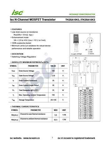
INCHANGE Semiconductor Isc N-Channel MOSFET Transistor TK25A10K3 ITK25A10K3 FEATURES Low drain-source on-resistance RDS(ON) = 31m (typ.) Enhancement mode Vth = 2.0 to 4.0V (VDS = 10 V, ID=1mA) 100% avalanche tested Minimum Lot-to-Lot variations for robust device performance and reliable operation DESCRITION Switching Voltage Regulators ABSOLUTE MAXIMUM RATIN
0.19. Size:253K inchange semiconductor
tk25a60x5.pdf
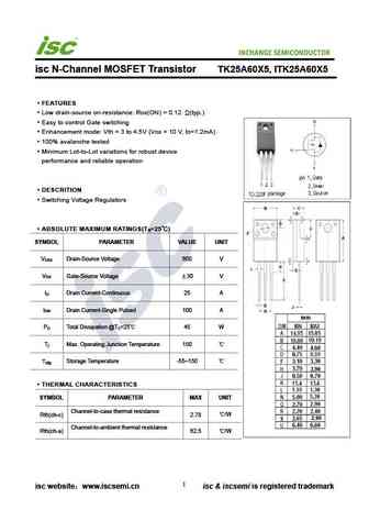
INCHANGE Semiconductor isc N-Channel MOSFET Transistor TK25A60X5, ITK25A60X5 FEATURES Low drain-source on-resistance RDS(ON) = 0.12 (typ.) Easy to control Gate switching Enhancement mode Vth = 3 to 4.5V (VDS = 10 V, ID=1.2mA) 100% avalanche tested Minimum Lot-to-Lot variations for robust device performance and reliable operation DESCRITION Switching Voltage Regula
0.20. Size:246K inchange semiconductor
tk25e60x5.pdf
INCHANGE Semiconductor isc N-Channel MOSFET Transistor TK25E60X5 ITK25E60X5 FEATURES Low drain-source on-resistance RDS(on) 0.14 . Enhancement mode Vth =3.0 to 4.5V (VDS = 10 V, ID=1.2mA) 100% avalanche tested Minimum Lot-to-Lot variations for robust device performance and reliable operation DESCRITION Switching Voltage Regulators ABSOLUTE MAXIMUM RATINGS(T
Otros transistores... TK21B, TK21C, TK23, TK23A, TK23C, TK24, TK24B, TK24C, BC547, TK250A, TK251A, TK252A, TK253A, TK254A, TK255A, TK256A, TK257A