TK25 Datasheet. Specs and Replacement
Type Designator: TK25 📄📄
Material of Transistor: Ge
Polarity: PNP
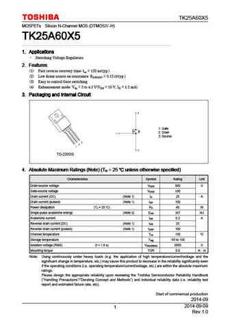
Absolute Maximum Ratings
Maximum Collector Power Dissipation (Pc): 0.2 W
Maximum Collector-Base Voltage |Vcb|: 20 V
Maximum Collector-Emitter Voltage |Vce|: 6 V
Maximum Emitter-Base Voltage |Veb|: 20 V
Maximum Collector Current |Ic max|: 0.25 A
Max. Operating Junction Temperature (Tj): 75 °C
Electrical Characteristics
Transition Frequency (ft): 6 MHz
Forward Current Transfer Ratio (hFE), MIN: 20
Noise Figure, dB: -
Package: X18
- BJT ⓘ Cross-Reference Search
TK25 datasheet
0.1. Size:219K toshiba
tk25a20d.pdf 
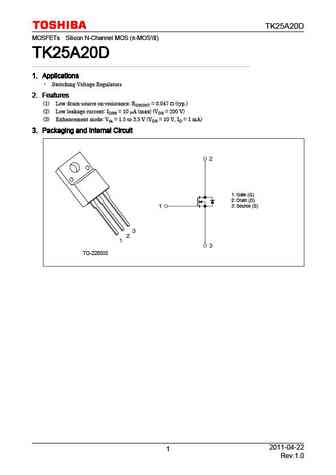
TK25A20D MOSFETs Silicon N-Channel MOS ( -MOS ) TK25A20D TK25A20D TK25A20D TK25A20D 1. Applications 1. Applications 1. Applications 1. Applications Switching Voltage Regulators 2. Features 2. Features 2. Features 2. Features (1) Low drain-source on-resistance RDS(ON) = 0.047 (typ.) (2) Low leakage current IDSS = 10 A (max) (VDS = 200 V) (3) Enhancement mode Vth ... See More ⇒
0.2. Size:236K toshiba
tk25a60x.pdf

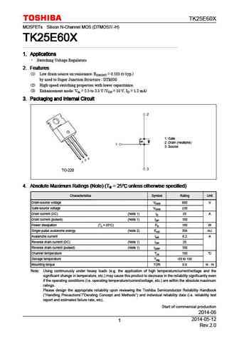
TK25A60X MOSFETs Silicon N-Channel MOS (DTMOS -H) TK25A60X TK25A60X TK25A60X TK25A60X 1. Applications 1. Applications 1. Applications 1. Applications Switching Voltage Regulators 2. Features 2. Features 2. Features 2. Features (1) Low drain-source on-resistance RDS(ON) = 0.105 (typ.) by used to Super Junction Structure DTMOS (2) High-speed switching properties wit... See More ⇒
0.3. Size:247K toshiba
tk25e60x.pdf
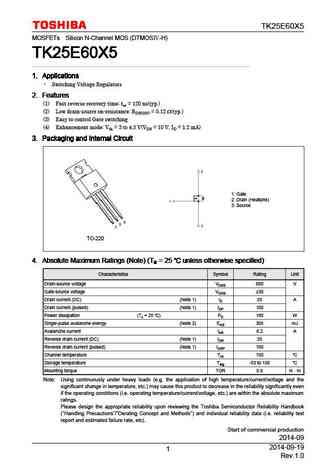
TK25E60X MOSFETs Silicon N-Channel MOS (DTMOS -H) TK25E60X TK25E60X TK25E60X TK25E60X 1. Applications 1. Applications 1. Applications 1. Applications Switching Voltage Regulators 2. Features 2. Features 2. Features 2. Features (1) Low drain-source on-resistance RDS(ON) = 0.105 (typ.) by used to Super Junction Structure DTMOS (2) High-speed switching properties wit... See More ⇒
0.4. Size:370K toshiba
tk25n60x5.pdf

TK25N60X5 MOSFETs Silicon N-Channel MOS (DTMOS -H) TK25N60X5 TK25N60X5 TK25N60X5 TK25N60X5 1. Applications 1. Applications 1. Applications 1. Applications Switching Voltage Regulators 2. Features 2. Features 2. Features 2. Features (1) Fast reverse recovery time trr = 120 ns(typ.) (2) Low drain-source on-resistance RDS(ON) = 0.12 (typ.) (3) Easy to control Gate switc... See More ⇒
0.5. Size:305K toshiba
tk25a10k3.pdf
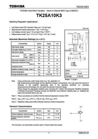
TK25A10K3 TOSHIBA Field Effect Transistor Silicon N Channel MOS Type (U-MOSIV) TK25A10K3 Swiching Regulator Applications Low drain-source ON resistance RDS (ON) = 31 m (typ.) Unit mm High forward transfer admittance Yfs = 50 S (typ.) Low leakage current IDSS = 10 A (max) (VDS = 100 V) Enhancement-model Vth = 2.0 to 4.0 V (VDS = 10 V, ID = 1 mA) Absolu... See More ⇒
0.6. Size:238K toshiba
tk25v60x.pdf

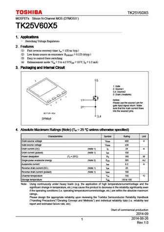
TK25V60X MOSFETs Silicon N-Channel MOS (DTMOS -H) TK25V60X TK25V60X TK25V60X TK25V60X 1. Applications 1. Applications 1. Applications 1. Applications Switching Voltage Regulators 2. Features 2. Features 2. Features 2. Features (1) Low drain-source on-resistance RDS(ON) = 0.11 (typ.) by used to Super Junction Structure DTMOS (2) High-speed switching properties with... See More ⇒
0.7. Size:244K toshiba
tk25n60x.pdf

TK25N60X MOSFETs Silicon N-Channel MOS (DTMOS -H) TK25N60X TK25N60X TK25N60X TK25N60X 1. Applications 1. Applications 1. Applications 1. Applications Switching Voltage Regulators 2. Features 2. Features 2. Features 2. Features (1) Low drain-source on-resistance RDS(ON) = 0.105 (typ.) by used to Super Junction Structure DTMOS (2) High-speed switching properties wit... See More ⇒
0.8. Size:363K toshiba
tk25a60x5.pdf
TK25A60X5 MOSFETs Silicon N-Channel MOS (DTMOS -H) TK25A60X5 TK25A60X5 TK25A60X5 TK25A60X5 1. Applications 1. Applications 1. Applications 1. Applications Switching Voltage Regulators 2. Features 2. Features 2. Features 2. Features (1) Fast reverse recovery time trr = 120 ns(typ.) (2) Low drain-source on-resistance RDS(ON) = 0.12 (typ.) (3) Easy to control Gate switc... See More ⇒
0.9. Size:365K toshiba
tk25v60x5.pdf
TK25V60X5 MOSFETs Silicon N-Channel MOS (DTMOS ) TK25V60X5 TK25V60X5 TK25V60X5 TK25V60X5 1. Applications 1. Applications 1. Applications 1. Applications Switching Voltage Regulators 2. Features 2. Features 2. Features 2. Features (1) Fast reverse recovery time trr = 120 ns (typ.) (2) Low drain-source on-resistance RDS(ON) = 0.125 (typ.) (3) Easy to control Gate switc... See More ⇒
0.10. Size:373K toshiba
tk25e60x5.pdf
TK25E60X5 MOSFETs Silicon N-Channel MOS (DTMOS -H) TK25E60X5 TK25E60X5 TK25E60X5 TK25E60X5 1. Applications 1. Applications 1. Applications 1. Applications Switching Voltage Regulators 2. Features 2. Features 2. Features 2. Features (1) Fast reverse recovery time trr = 120 ns(typ.) (2) Low drain-source on-resistance RDS(ON) = 0.12 (typ.) (3) Easy to control Gate switc... See More ⇒
0.11. Size:241K toshiba
tk25s06n1l.pdf
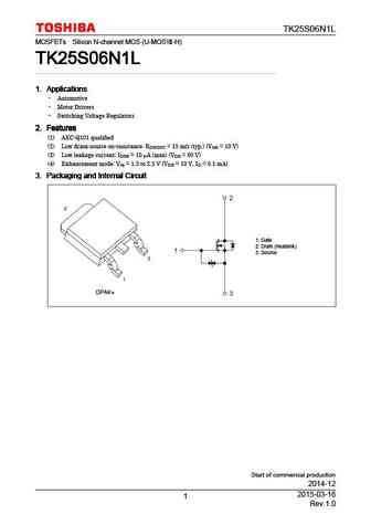
TK25S06N1L MOSFETs Silicon N-channel MOS (U-MOS -H) TK25S06N1L TK25S06N1L TK25S06N1L TK25S06N1L 1. Applications 1. Applications 1. Applications 1. Applications Automotive Motor Drivers Switching Voltage Regulators 2. Features 2. Features 2. Features 2. Features (1) AEC-Q101 qualified (2) Low drain-source on-resistance RDS(ON) = 15 m (typ.) (VGS = 10 V) (3) L... See More ⇒
0.12. Size:560K ixys
ixtk250n10.pdf
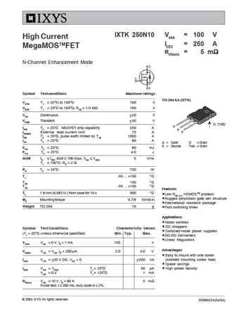
IXTK 250N10 VDSS = 100 V High Current ID25 = 250 A MegaMOSTMFET RDS(on) = 5 m N-Channel Enhancement Mode Symbol Test conditions Maximum ratings TO-264 AA (IXTK) VDSS TJ = 25 C to 150 C 100 V VDGR TJ = 25 C to 150 C; RGS = 1.0 M 100 V VGS Continuous 20 V VGSM Transient 30 V D (TAB) G ID25 TC = 25 C MOSFET chip capability 250 A D ID(RMS) Externa... See More ⇒
0.13. Size:232K lrc
lntk2575lt1g s-lntk2575lt1g.pdf
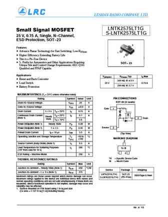
LESHAN RADIO COMPANY, LTD. LNTK2575LT1G Small Signal MOSFET S-LNTK2575LT1G 25 V, 0.75 A, Single, N-Channel, ESD Protection, SOT-23 3 Features Advance Planar Technology for Fast Switching, Low RDS(on) 1 Higher Efficiency Extending Battery Life 2 This is a Pb-Free Device S- Prefix for Automotive and Other Applications Requiring SOT 23 Unique Site and Control Ch... See More ⇒
0.14. Size:430K first silicon
ftk25n03pdfn33.pdf
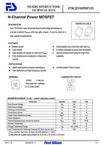
SEMICONDUCTOR FTK25N03PDFN33 TECHNICAL DATA N-Channel Power MOSFET PDFN3.3 3.3-8L-A DESCRIPTION The FTK25N03 uses advanced trench technology and design to provide excellent RDS(ON) with low gate charge. It can be used in a wide variety of applications FEATURES Battery switch Good stability and uniformity with high EAS Load switch Excellent package for good he... See More ⇒
0.15. Size:252K inchange semiconductor
tk25a20d.pdf
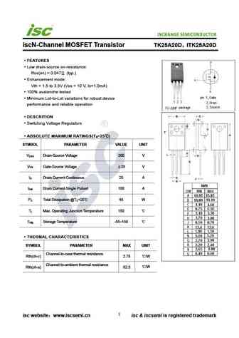
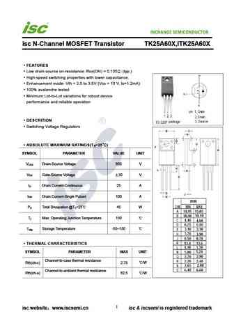
INCHANGE Semiconductor iscN-Channel MOSFET Transistor TK25A20D ITK25A20D FEATURES Low drain-source on-resistance RDS(on) = 0.047 (typ.) Enhancement mode Vth = 1.5 to 3.5V (VDS = 10 V, ID=1.0mA) 100% avalanche tested Minimum Lot-to-Lot variations for robust device performance and reliable operation DESCRITION Switching Voltage Regulators ABSOLUTE MAXIMUM RATING... See More ⇒
0.17. Size:246K inchange semiconductor
tk25e60x.pdf
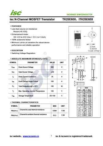
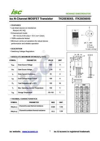
INCHANGE Semiconductor isc N-Channel MOSFET Transistor TK25E60X ITK25E60X FEATURES Low drain-source on-resistance RDS(on) 0.125 . Enhancement mode Vth =2.5 to 3.5V (VDS = 10 V, ID=1.2mA) 100% avalanche tested Minimum Lot-to-Lot variations for robust device performance and reliable operation DESCRITION Switching Voltage Regulators ABSOLUTE MAXIMUM RATINGS(T =... See More ⇒
0.18. Size:252K inchange semiconductor
tk25a10k3.pdf
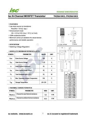
INCHANGE Semiconductor Isc N-Channel MOSFET Transistor TK25A10K3 ITK25A10K3 FEATURES Low drain-source on-resistance RDS(ON) = 31m (typ.) Enhancement mode Vth = 2.0 to 4.0V (VDS = 10 V, ID=1mA) 100% avalanche tested Minimum Lot-to-Lot variations for robust device performance and reliable operation DESCRITION Switching Voltage Regulators ABSOLUTE MAXIMUM RATIN... See More ⇒
0.19. Size:253K inchange semiconductor
tk25a60x5.pdf
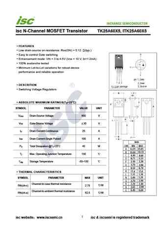
INCHANGE Semiconductor isc N-Channel MOSFET Transistor TK25A60X5, ITK25A60X5 FEATURES Low drain-source on-resistance RDS(ON) = 0.12 (typ.) Easy to control Gate switching Enhancement mode Vth = 3 to 4.5V (VDS = 10 V, ID=1.2mA) 100% avalanche tested Minimum Lot-to-Lot variations for robust device performance and reliable operation DESCRITION Switching Voltage Regula... See More ⇒
0.20. Size:246K inchange semiconductor
tk25e60x5.pdf
INCHANGE Semiconductor isc N-Channel MOSFET Transistor TK25E60X5 ITK25E60X5 FEATURES Low drain-source on-resistance RDS(on) 0.14 . Enhancement mode Vth =3.0 to 4.5V (VDS = 10 V, ID=1.2mA) 100% avalanche tested Minimum Lot-to-Lot variations for robust device performance and reliable operation DESCRITION Switching Voltage Regulators ABSOLUTE MAXIMUM RATINGS(T ... See More ⇒
Detailed specifications: TK21B, TK21C, TK23, TK23A, TK23C, TK24, TK24B, TK24C, BC547, TK250A, TK251A, TK252A, TK253A, TK254A, TK255A, TK256A, TK257A
Keywords - TK25 pdf specs
TK25 cross reference
TK25 equivalent finder
TK25 pdf lookup
TK25 substitution
TK25 replacement