TK30 Datasheet. Equivalente. Reemplazo. Hoja de especificaciones. Principales características
Número de Parte: TK30 📄📄
Material: Ge
Polaridad de transistor: PNP
ESPECIFICACIONES MÁXIMAS
Disipación total del dispositivo (Pc): 0.2 W
Tensión colector-base (Vcb): 30 V
Tensión colector-emisor (Vce): 10 V
Tensión emisor-base (Veb): 30 V
Corriente del colector DC máxima (Ic): 0.1 A
Temperatura operativa máxima (Tj): 75 °C
CARACTERÍSTICAS ELÉCTRICAS
Transición de frecuencia (fT): 3 MHz
Ganancia de corriente contínua (hFE): 20
Encapsulados: X18
📄📄 Copiar
Búsqueda de reemplazo de TK30
- Selecciónⓘ de transistores por parámetros
TK30 datasheet
0.2. Size:332K st
stk30n2llh5.pdf 
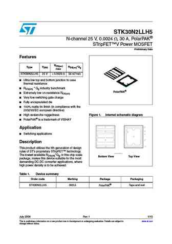
STK30N2LLH5 N-channel 25 V, 0.0024 , 30 A, PolarPAK STripFET V Power MOSFET Preliminary Data Features RDS(on) VDSS RDS(on)*Qg Type max STK30N2LLH5 25 V
0.3. Size:230K toshiba
tk30j25d.pdf

TK30J25D MOSFETs Silicon N-Channel MOS ( -MOS ) TK30J25D TK30J25D TK30J25D TK30J25D 1. Applications 1. Applications 1. Applications 1. Applications Switching Voltage Regulators 2. Features 2. Features 2. Features 2. Features (1) Low drain-source on-resistance RDS(ON) = 0.046 (typ.) (2) Low leakage current IDSS = 10 A (max) (VDS = 250 V) (3) Enhancement mode Vth
0.4. Size:237K toshiba
tk30a06n1.pdf
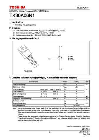
TK30A06N1 MOSFETs Silicon N-channel MOS (U-MOS -H) TK30A06N1 TK30A06N1 TK30A06N1 TK30A06N1 1. Applications 1. Applications 1. Applications 1. Applications Switching Voltage Regulators 2. Features 2. Features 2. Features 2. Features (1) Low drain-source on-resistance RDS(ON) = 12.2 m (typ.) (VGS = 10 V) (2) Low leakage current IDSS = 10 A (max) (VDS = 60 V) (3) Enha
0.5. Size:196K toshiba
tk30a06j3a.pdf
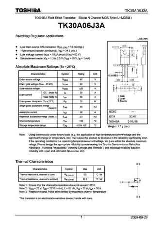
TK30A06J3A TOSHIBA Field Effect Transistor Silicon N Channel MOS Type (U-MOS ) TK30A06J3A Switching Regulator Applications Unit mm Low drain-source ON-resistance RDS (ON) = 19 m (typ.) High forward transfer admittance Yfs = 34 S (typ.) Low leakage current IDSS = 10 A (max) (VDS = 60 V) Enhancement mode Vth = 1.3 to 2.5 V (VDS = 10 V, ID = 1 mA) Absolute M
0.6. Size:246K toshiba
tk30e06n1.pdf
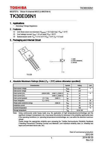
TK30E06N1 MOSFETs Silicon N-channel MOS (U-MOS -H) TK30E06N1 TK30E06N1 TK30E06N1 TK30E06N1 1. Applications 1. Applications 1. Applications 1. Applications Switching Voltage Regulators 2. Features 2. Features 2. Features 2. Features (1) Low drain-source on-resistance RDS(ON) = 12.2 m (typ.) (VGS = 10 V) (2) Low leakage current IDSS = 10 A (max) (VDS = 60 V) (3) Enha
0.7. Size:251K toshiba
tk30s06k3l.pdf
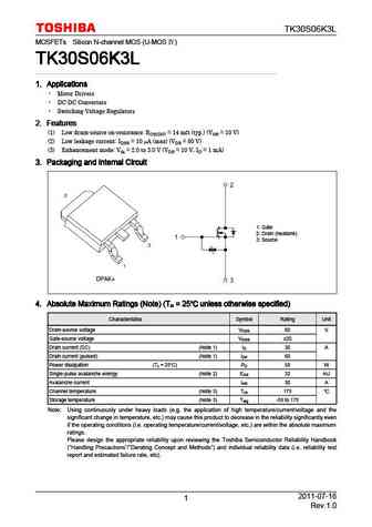
TK30S06K3L MOSFETs Silicon N-channel MOS (U-MOS ) TK30S06K3L TK30S06K3L TK30S06K3L TK30S06K3L 1. Applications 1. Applications 1. Applications 1. Applications Motor Drivers DC-DC Converters Switching Voltage Regulators 2. Features 2. Features 2. Features 2. Features (1) Low drain-source on-resistance RDS(ON) = 14 m (typ.) (VGS = 10 V) (2) Low leakage current
0.8. Size:54K onsemi
ntk3043n-d ntk3043nat5g ntk3043nt1g.pdf
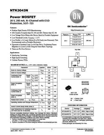
NTK3043N Power MOSFET 20 V, 285 mA, N-Channel with ESD Protection, SOT-723 Features http //onsemi.com Enables High Density PCB Manufacturing 44% Smaller Footprint than SC-89 and 38% Thinner than SC-89 V(BR)DSS RDS(on) TYP ID Max Low Voltage Drive Makes this Device Ideal for Portable Equipment 1.5 W @ 4.5 V Low Threshold Levels, VGS(TH)
0.9. Size:128K onsemi
ntk3043n.pdf
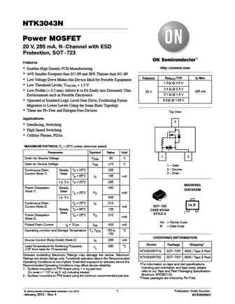
NTK3043N Power MOSFET 20 V, 285 mA, N-Channel with ESD Protection, SOT-723 Features http //onsemi.com Enables High Density PCB Manufacturing 44% Smaller Footprint than SC-89 and 38% Thinner than SC-89 V(BR)DSS RDS(on) TYP ID Max Low Voltage Drive Makes this Device Ideal for Portable Equipment 1.5 W @ 4.5 V Low Threshold Levels, VGS(TH)
0.10. Size:229K lrc
lntk3043pt5g s-lntk3043pt5g.pdf
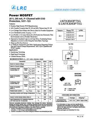
LESHAN RADIO COMPANY, LTD. Power MOSFET 20 V, 285 mA, P-Channel with ESD Protection, SOT-723 LNTK3043PT5G Features S-LNTK3043PT5G Enables High Density PCB Manufacturing 44% Smaller Footprint than SC-89 and 38% Thinner than SC-89 V(BR)DSS RDS(on) TYP ID Max Low Voltage Drive Makes this Device Ideal for Portable Equipment 1.5 W @ 4.5 V Low Threshold Levels, VGS(TH)
0.11. Size:304K first silicon
ftk3018.pdf
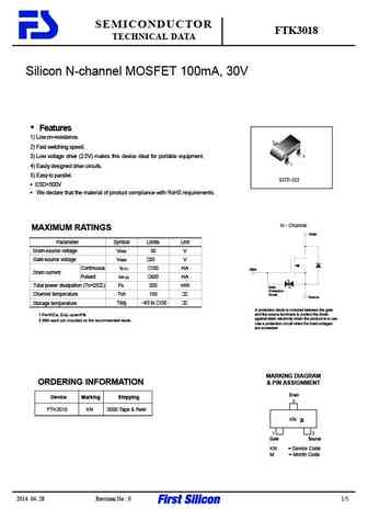
SEMICONDUCTOR FTK3018 TECHNICAL DATA Silicon N-channel MOSFET 100mA, 30V Features 1) Low on-resistance. 3 2) Fast switching speed. 2 3) Low voltage drive (2.5V) makes this device ideal for portable equipment. 1 4) Easily designed drive circuits. 5) Easy to parallel. SOT 323 ESD>500V We declare that the material of product compliance with RoHS requirements. N
0.12. Size:250K first silicon
ftk3004d.pdf
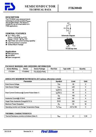
SEMICONDUCTOR FTK3004D TECHNICAL DATA DESCRIPTION The FTK3004D uses advanced trench technology to provide excellent RDS(ON) and low gate charge .This device is D suitable for use as a load switch or in PWM applications. G GENERAL FEATURES S VDS = 30V,ID =55A Schematic diagram RDS(ON)
0.13. Size:421K first silicon
ftk3051.pdf
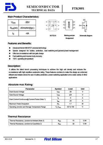
SEMICONDUCTOR FTK3051 TECHNICAL DATA Main Product Characteristics D 1 6 D D VDSS -30V 2 5 D D G RDS(on) 45mohm(typ.) 3 4 G S S ID -4A SOT23-6 Marking and pin Schematic diagram A ssignment Features and Benefits Advanced trench MOSFET process technology Special designed for buttery protection, load switching and general power management Ultra low on-resista
0.14. Size:315K first silicon
ftk3022.pdf
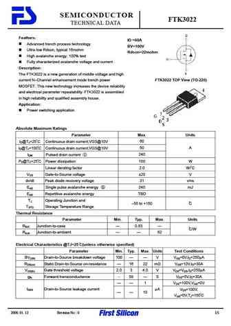
SEMICONDUCTOR FTK3022 TECHNICAL DATA Feathers ID =60A Advanced trench process technology BV=100V Ultra low Rdson, typical 16mohm Rdson=22mohm High avalanche energy, 100% test Fully characterized avalanche voltage and current Description The FTK3022 is a new generation of middle voltage and high current N Channel enhancement mode trench power FTK3022 TOP View (TO
0.15. Size:1287K jiejie micro
jmtk3006d.pdf
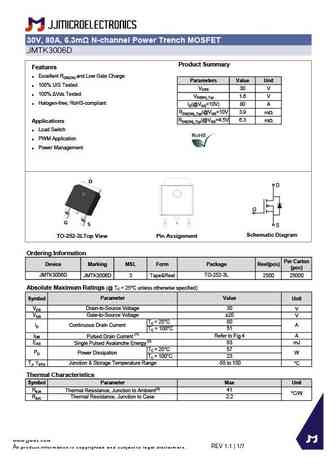
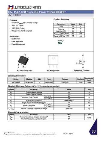
30V, 80A, 6.3m N-channel Power Trench MOSFET JMTK3006D Product Summary Features Excellent RDS(ON) and Low Gate Charge Parameters Value Unit 100% UIS Tested VDSS 30 V 100% Vds Tested VGS(th)_Typ 1.6 V Halogen-free; RoHS-compliant ID(@VGS=10V) 80 A RDS(ON)_Typ(@VGS=10V 3.9 mW RDS(ON)_Typ(@VGS=4.5V 6.3 mW Applications Load Switch PWM Application Pow
0.16. Size:1076K jiejie micro
jmtk3005a.pdf
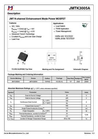
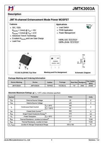
JMTK3005A Description JMT N-channel Enhancement Mode Power MOSFET Features Applications Load Switch 30V, 100A PWM Application RDS(ON)
0.17. Size:884K jiejie micro
jmtk3006b.pdf
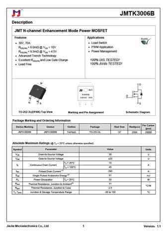
JMTK3006B Description JMT N-channel Enhancement Mode Power MOSFET Features Applications 30V, 70A Load Switch RDS(ON)
0.18. Size:1287K jiejie micro
jmtk3005b.pdf
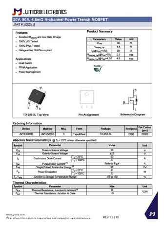
30V, 90A, 4.6m N-channel Power Trench MOSFET JMTK3005B Product Summary Features Excellent RDS(ON) and Low Gate Charge Parameters Value Unit 100% UIS Tested VDSS 30 V 100% Vds Tested VGS(th)_Typ 1.6 V Halogen-free; RoHS-compliant ID(@VGS=10V) 90 A RDS(ON)_Typ(@VGS=10V 2.9 mW RDS(ON)_Typ(@VGS=4.5V 4.6 mW Applications Load Switch PWM Application Pow
0.19. Size:982K jiejie micro
jmtk3002b.pdf
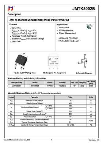
JMTK3002B Description JMT N-channel Enhancement Mode Power MOSFET Features Applications 30V, 180A Load Switch RDS(ON)
0.20. Size:1292K jiejie micro
jmtk3006c.pdf
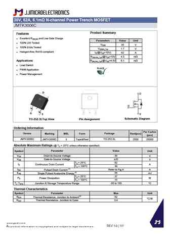
30V, 62A, 6.1m N-channel Power Trench MOSFET JMTK3006C Product Summary Features Excellent RDS(ON) and Low Gate Charge Parameters Value Unit 100% UIS Tested VDSS 30 V 100% Vds Tested VGS(th)_Typ 1.7 V Halogen-free; RoHS-compliant ID(@VGS=10V) 62 A RDS(ON)_Typ(@VGS=10V 4.3 mW Applications RDS(ON)_Typ(@VGS=4.5V 6.1 mW Load Switch PWM Application Pow
0.21. Size:881K jiejie micro
jmtk3004a.pdf
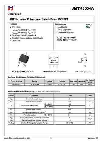
JMTK3004A Description JMT N-channel Enhancement Mode Power MOSFET Features Applications 30V, 100A Load Switch RDS(ON)
0.22. Size:1287K jiejie micro
jmtk3006e.pdf
30V, 61A,7.0m N-channel Power Trench MOSFET JMTK3006E Product Summary Features Excellent RDS(ON) and Low Gate Charge Parameters Value Unit 100% UIS Tested VDSS 30 V 100% Vds Tested VGS(th)_Typ 1.4 V Halogen-free; RoHS-compliant ID(@VGS=10V) 61 A RDS(ON)_Typ(@VGS=10V 4.3 mW RDS(ON)_Typ(@VGS=4.5V 7.0 mW Applications Load Switch PWM Application Powe
0.23. Size:968K jiejie micro
jmtk3003a.pdf
JMTK3003A Description JMT N-channel Enhancement Mode Power MOSFET Features Applications 30V, 150A Load Switch RDS(ON)
0.24. Size:1254K jiejie micro
jmtk3005c.pdf
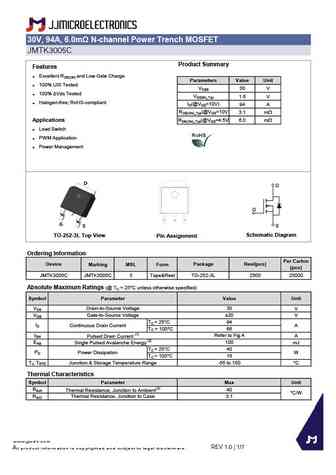
30V, 94A, 6.0m N-channel Power Trench MOSFET JMTK3005C Product Summary Features Excellent RDS(ON) and Low Gate Charge Parameters Value Unit 100% UIS Tested VDSS 30 V 100% Vds Tested VGS(th)_Typ 1.6 V Halogen-free; RoHS-compliant ID(@VGS=10V) 94 A RDS(ON)_Typ(@VGS=10V 3.1 mW Applications RDS(ON)_Typ(@VGS=4.5V 6.0 mW Load Switch PWM Application Pow
0.25. Size:576K jiejie micro
jmtk3005l.pdf

JMTK3005L Description JMT N-channel MOSFET Features Application 30V, 90A Load Switch R
0.26. Size:2018K cn vbsemi
tk30a06j3.pdf
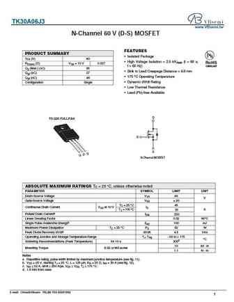
TK30A06J3 www.VBsemi.tw N-Channel 60 V (D-S) MOSFET FEATURES PRODUCT SUMMARY Isolated Package VDS (V) 60 High Voltage Isolation = 2.5 kVRMS (t = 60 s; RoHS RDS(on) ( )VGS = 10 V 0.027 f = 60 Hz) COMPLIANT Qg (Max.) (nC) 95 Sink to Lead Creepage Distance = 4.8 mm Qgs (nC) 27 175 C Operating Temperature Qgd (nC) 46 Dynamic dV/dt Rating Configuration Single
0.27. Size:253K inchange semiconductor
tk30a06n1.pdf
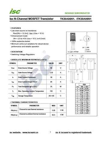
INCHANGE Semiconductor Isc N-Channel MOSFET Transistor TK30A06N1 ITK30A06N1 FEATURES Low drain-source on-resistance RDS(ON) = 12.2m (typ.) (VGS = 10 V) Enhancement mode Vth = 2.0 to 4.0V (VDS = 10 V, ID=0.2mA) 100% avalanche tested Minimum Lot-to-Lot variations for robust device performance and reliable operation DESCRITION Switching Voltage Regulators ABSOLUT
0.28. Size:246K inchange semiconductor
tk30e06n1.pdf
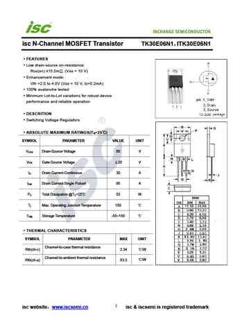
INCHANGE Semiconductor isc N-Channel MOSFET Transistor TK30E06N1 ITK30E06N1 FEATURES Low drain-source on-resistance RDS(on) 15.0m . (VGS = 10 V) Enhancement mode Vth =2.0 to 4.0V (VDS = 10 V, ID=0.2mA) 100% avalanche tested Minimum Lot-to-Lot variations for robust device performance and reliable operation DESCRITION Switching Voltage Regulators ABSOLUTE MA
Otros transistores... TK257A, TK258A, TK259A, TK25B, TK25C, TK264A, TK28, TK28C, 2SA1943, TK30D, TK31, TK31D, TK33, TK33C, TK34, TK34C, TK35