TK30 Specs and Replacement
Type Designator: TK30
Material of Transistor: Ge
Polarity: PNP
Absolute Maximum Ratings
Maximum Collector Power Dissipation (Pc): 0.2
W
Maximum Collector-Base Voltage |Vcb|: 30
V
Maximum Collector-Emitter Voltage |Vce|: 10
V
Maximum Emitter-Base Voltage |Veb|: 30
V
Maximum Collector Current |Ic max|: 0.1
A
Max. Operating Junction Temperature (Tj): 75
°C
Electrical Characteristics
Transition Frequency (ft): 3
MHz
Forward Current Transfer Ratio (hFE), MIN: 20
Noise Figure, dB: -
Package: X18
-
BJT ⓘ Cross-Reference Search
TK30 datasheet
0.2. Size:332K st
stk30n2llh5.pdf 
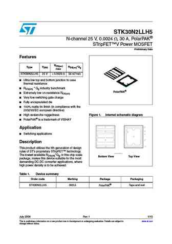
STK30N2LLH5 N-channel 25 V, 0.0024 , 30 A, PolarPAK STripFET V Power MOSFET Preliminary Data Features RDS(on) VDSS RDS(on)*Qg Type max STK30N2LLH5 25 V ... See More ⇒
0.3. Size:230K toshiba
tk30j25d.pdf

TK30J25D MOSFETs Silicon N-Channel MOS ( -MOS ) TK30J25D TK30J25D TK30J25D TK30J25D 1. Applications 1. Applications 1. Applications 1. Applications Switching Voltage Regulators 2. Features 2. Features 2. Features 2. Features (1) Low drain-source on-resistance RDS(ON) = 0.046 (typ.) (2) Low leakage current IDSS = 10 A (max) (VDS = 250 V) (3) Enhancement mode Vth ... See More ⇒
0.4. Size:237K toshiba
tk30a06n1.pdf
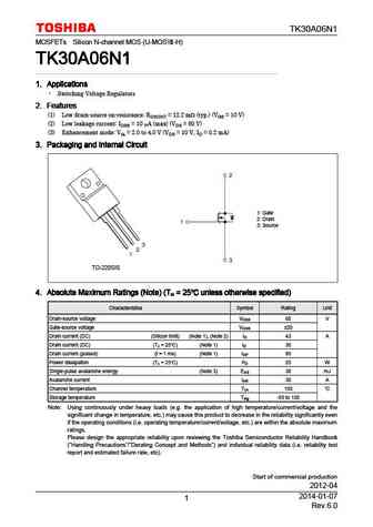
TK30A06N1 MOSFETs Silicon N-channel MOS (U-MOS -H) TK30A06N1 TK30A06N1 TK30A06N1 TK30A06N1 1. Applications 1. Applications 1. Applications 1. Applications Switching Voltage Regulators 2. Features 2. Features 2. Features 2. Features (1) Low drain-source on-resistance RDS(ON) = 12.2 m (typ.) (VGS = 10 V) (2) Low leakage current IDSS = 10 A (max) (VDS = 60 V) (3) Enha... See More ⇒
0.5. Size:196K toshiba
tk30a06j3a.pdf
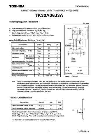
TK30A06J3A TOSHIBA Field Effect Transistor Silicon N Channel MOS Type (U-MOS ) TK30A06J3A Switching Regulator Applications Unit mm Low drain-source ON-resistance RDS (ON) = 19 m (typ.) High forward transfer admittance Yfs = 34 S (typ.) Low leakage current IDSS = 10 A (max) (VDS = 60 V) Enhancement mode Vth = 1.3 to 2.5 V (VDS = 10 V, ID = 1 mA) Absolute M... See More ⇒
0.6. Size:246K toshiba
tk30e06n1.pdf
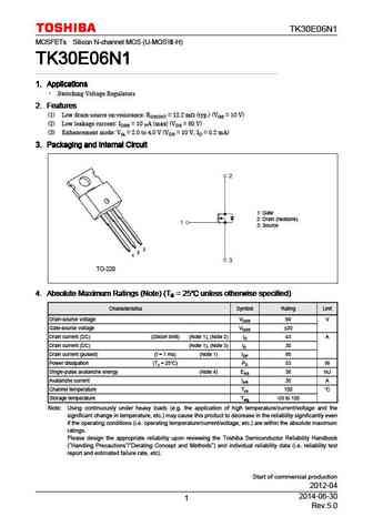
TK30E06N1 MOSFETs Silicon N-channel MOS (U-MOS -H) TK30E06N1 TK30E06N1 TK30E06N1 TK30E06N1 1. Applications 1. Applications 1. Applications 1. Applications Switching Voltage Regulators 2. Features 2. Features 2. Features 2. Features (1) Low drain-source on-resistance RDS(ON) = 12.2 m (typ.) (VGS = 10 V) (2) Low leakage current IDSS = 10 A (max) (VDS = 60 V) (3) Enha... See More ⇒
0.7. Size:251K toshiba
tk30s06k3l.pdf
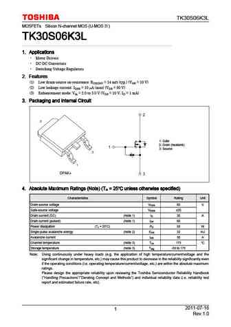
TK30S06K3L MOSFETs Silicon N-channel MOS (U-MOS ) TK30S06K3L TK30S06K3L TK30S06K3L TK30S06K3L 1. Applications 1. Applications 1. Applications 1. Applications Motor Drivers DC-DC Converters Switching Voltage Regulators 2. Features 2. Features 2. Features 2. Features (1) Low drain-source on-resistance RDS(ON) = 14 m (typ.) (VGS = 10 V) (2) Low leakage current ... See More ⇒
0.8. Size:54K onsemi
ntk3043n-d ntk3043nat5g ntk3043nt1g.pdf
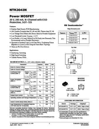
NTK3043N Power MOSFET 20 V, 285 mA, N-Channel with ESD Protection, SOT-723 Features http //onsemi.com Enables High Density PCB Manufacturing 44% Smaller Footprint than SC-89 and 38% Thinner than SC-89 V(BR)DSS RDS(on) TYP ID Max Low Voltage Drive Makes this Device Ideal for Portable Equipment 1.5 W @ 4.5 V Low Threshold Levels, VGS(TH) ... See More ⇒
0.9. Size:128K onsemi
ntk3043n.pdf
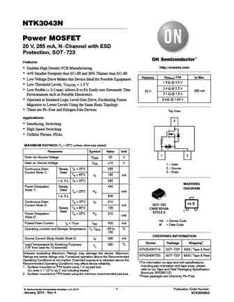
NTK3043N Power MOSFET 20 V, 285 mA, N-Channel with ESD Protection, SOT-723 Features http //onsemi.com Enables High Density PCB Manufacturing 44% Smaller Footprint than SC-89 and 38% Thinner than SC-89 V(BR)DSS RDS(on) TYP ID Max Low Voltage Drive Makes this Device Ideal for Portable Equipment 1.5 W @ 4.5 V Low Threshold Levels, VGS(TH) ... See More ⇒
0.10. Size:229K lrc
lntk3043pt5g s-lntk3043pt5g.pdf
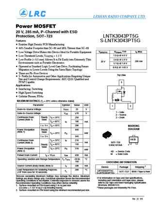
LESHAN RADIO COMPANY, LTD. Power MOSFET 20 V, 285 mA, P-Channel with ESD Protection, SOT-723 LNTK3043PT5G Features S-LNTK3043PT5G Enables High Density PCB Manufacturing 44% Smaller Footprint than SC-89 and 38% Thinner than SC-89 V(BR)DSS RDS(on) TYP ID Max Low Voltage Drive Makes this Device Ideal for Portable Equipment 1.5 W @ 4.5 V Low Threshold Levels, VGS(TH) ... See More ⇒
0.11. Size:304K first silicon
ftk3018.pdf
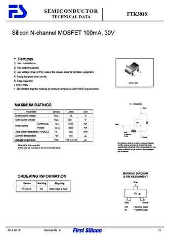
SEMICONDUCTOR FTK3018 TECHNICAL DATA Silicon N-channel MOSFET 100mA, 30V Features 1) Low on-resistance. 3 2) Fast switching speed. 2 3) Low voltage drive (2.5V) makes this device ideal for portable equipment. 1 4) Easily designed drive circuits. 5) Easy to parallel. SOT 323 ESD>500V We declare that the material of product compliance with RoHS requirements. N ... See More ⇒
0.12. Size:250K first silicon
ftk3004d.pdf
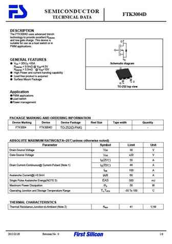
SEMICONDUCTOR FTK3004D TECHNICAL DATA DESCRIPTION The FTK3004D uses advanced trench technology to provide excellent RDS(ON) and low gate charge .This device is D suitable for use as a load switch or in PWM applications. G GENERAL FEATURES S VDS = 30V,ID =55A Schematic diagram RDS(ON) ... See More ⇒
0.13. Size:421K first silicon
ftk3051.pdf
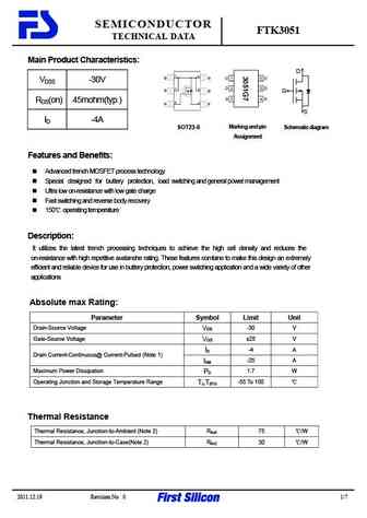
SEMICONDUCTOR FTK3051 TECHNICAL DATA Main Product Characteristics D 1 6 D D VDSS -30V 2 5 D D G RDS(on) 45mohm(typ.) 3 4 G S S ID -4A SOT23-6 Marking and pin Schematic diagram A ssignment Features and Benefits Advanced trench MOSFET process technology Special designed for buttery protection, load switching and general power management Ultra low on-resista... See More ⇒
0.14. Size:315K first silicon
ftk3022.pdf
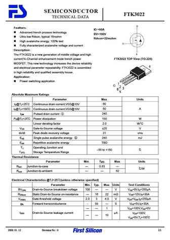
SEMICONDUCTOR FTK3022 TECHNICAL DATA Feathers ID =60A Advanced trench process technology BV=100V Ultra low Rdson, typical 16mohm Rdson=22mohm High avalanche energy, 100% test Fully characterized avalanche voltage and current Description The FTK3022 is a new generation of middle voltage and high current N Channel enhancement mode trench power FTK3022 TOP View (TO... See More ⇒
0.15. Size:1287K jiejie micro
jmtk3006d.pdf
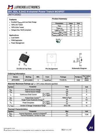
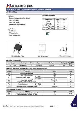
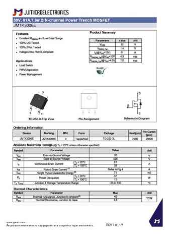
30V, 80A, 6.3m N-channel Power Trench MOSFET JMTK3006D Product Summary Features Excellent RDS(ON) and Low Gate Charge Parameters Value Unit 100% UIS Tested VDSS 30 V 100% Vds Tested VGS(th)_Typ 1.6 V Halogen-free; RoHS-compliant ID(@VGS=10V) 80 A RDS(ON)_Typ(@VGS=10V 3.9 mW RDS(ON)_Typ(@VGS=4.5V 6.3 mW Applications Load Switch PWM Application Pow... See More ⇒
0.16. Size:1076K jiejie micro
jmtk3005a.pdf
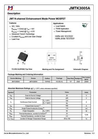
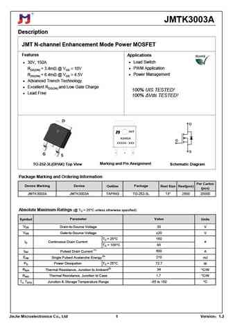
JMTK3005A Description JMT N-channel Enhancement Mode Power MOSFET Features Applications Load Switch 30V, 100A PWM Application RDS(ON) ... See More ⇒
0.17. Size:884K jiejie micro
jmtk3006b.pdf
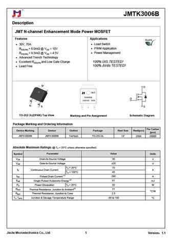
JMTK3006B Description JMT N-channel Enhancement Mode Power MOSFET Features Applications 30V, 70A Load Switch RDS(ON) ... See More ⇒
0.18. Size:1287K jiejie micro
jmtk3005b.pdf
30V, 90A, 4.6m N-channel Power Trench MOSFET JMTK3005B Product Summary Features Excellent RDS(ON) and Low Gate Charge Parameters Value Unit 100% UIS Tested VDSS 30 V 100% Vds Tested VGS(th)_Typ 1.6 V Halogen-free; RoHS-compliant ID(@VGS=10V) 90 A RDS(ON)_Typ(@VGS=10V 2.9 mW RDS(ON)_Typ(@VGS=4.5V 4.6 mW Applications Load Switch PWM Application Pow... See More ⇒
0.19. Size:982K jiejie micro
jmtk3002b.pdf
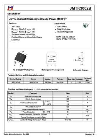
JMTK3002B Description JMT N-channel Enhancement Mode Power MOSFET Features Applications 30V, 180A Load Switch RDS(ON) ... See More ⇒
0.20. Size:1292K jiejie micro
jmtk3006c.pdf
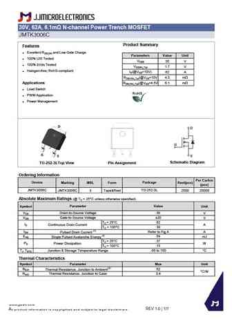
30V, 62A, 6.1m N-channel Power Trench MOSFET JMTK3006C Product Summary Features Excellent RDS(ON) and Low Gate Charge Parameters Value Unit 100% UIS Tested VDSS 30 V 100% Vds Tested VGS(th)_Typ 1.7 V Halogen-free; RoHS-compliant ID(@VGS=10V) 62 A RDS(ON)_Typ(@VGS=10V 4.3 mW Applications RDS(ON)_Typ(@VGS=4.5V 6.1 mW Load Switch PWM Application Pow... See More ⇒
0.21. Size:881K jiejie micro
jmtk3004a.pdf
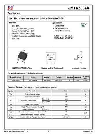
JMTK3004A Description JMT N-channel Enhancement Mode Power MOSFET Features Applications 30V, 100A Load Switch RDS(ON) ... See More ⇒
0.22. Size:1287K jiejie micro
jmtk3006e.pdf
30V, 61A,7.0m N-channel Power Trench MOSFET JMTK3006E Product Summary Features Excellent RDS(ON) and Low Gate Charge Parameters Value Unit 100% UIS Tested VDSS 30 V 100% Vds Tested VGS(th)_Typ 1.4 V Halogen-free; RoHS-compliant ID(@VGS=10V) 61 A RDS(ON)_Typ(@VGS=10V 4.3 mW RDS(ON)_Typ(@VGS=4.5V 7.0 mW Applications Load Switch PWM Application Powe... See More ⇒
0.23. Size:968K jiejie micro
jmtk3003a.pdf
JMTK3003A Description JMT N-channel Enhancement Mode Power MOSFET Features Applications 30V, 150A Load Switch RDS(ON) ... See More ⇒
0.24. Size:1254K jiejie micro
jmtk3005c.pdf
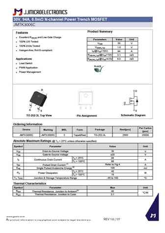
30V, 94A, 6.0m N-channel Power Trench MOSFET JMTK3005C Product Summary Features Excellent RDS(ON) and Low Gate Charge Parameters Value Unit 100% UIS Tested VDSS 30 V 100% Vds Tested VGS(th)_Typ 1.6 V Halogen-free; RoHS-compliant ID(@VGS=10V) 94 A RDS(ON)_Typ(@VGS=10V 3.1 mW Applications RDS(ON)_Typ(@VGS=4.5V 6.0 mW Load Switch PWM Application Pow... See More ⇒
0.25. Size:576K jiejie micro
jmtk3005l.pdf
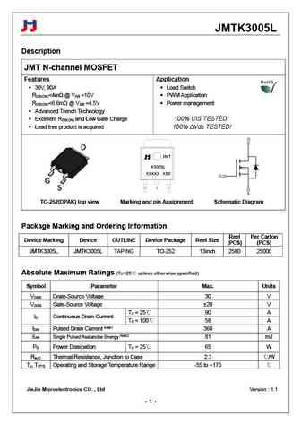
JMTK3005L Description JMT N-channel MOSFET Features Application 30V, 90A Load Switch R ... See More ⇒
0.26. Size:2018K cn vbsemi
tk30a06j3.pdf
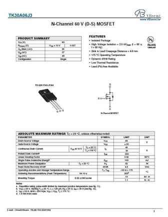
TK30A06J3 www.VBsemi.tw N-Channel 60 V (D-S) MOSFET FEATURES PRODUCT SUMMARY Isolated Package VDS (V) 60 High Voltage Isolation = 2.5 kVRMS (t = 60 s; RoHS RDS(on) ( )VGS = 10 V 0.027 f = 60 Hz) COMPLIANT Qg (Max.) (nC) 95 Sink to Lead Creepage Distance = 4.8 mm Qgs (nC) 27 175 C Operating Temperature Qgd (nC) 46 Dynamic dV/dt Rating Configuration Single ... See More ⇒
0.27. Size:253K inchange semiconductor
tk30a06n1.pdf
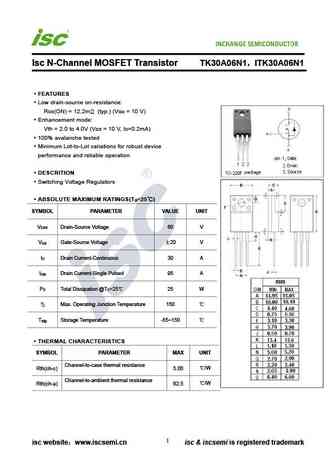
INCHANGE Semiconductor Isc N-Channel MOSFET Transistor TK30A06N1 ITK30A06N1 FEATURES Low drain-source on-resistance RDS(ON) = 12.2m (typ.) (VGS = 10 V) Enhancement mode Vth = 2.0 to 4.0V (VDS = 10 V, ID=0.2mA) 100% avalanche tested Minimum Lot-to-Lot variations for robust device performance and reliable operation DESCRITION Switching Voltage Regulators ABSOLUT... See More ⇒
0.28. Size:246K inchange semiconductor
tk30e06n1.pdf
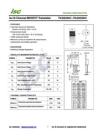
INCHANGE Semiconductor isc N-Channel MOSFET Transistor TK30E06N1 ITK30E06N1 FEATURES Low drain-source on-resistance RDS(on) 15.0m . (VGS = 10 V) Enhancement mode Vth =2.0 to 4.0V (VDS = 10 V, ID=0.2mA) 100% avalanche tested Minimum Lot-to-Lot variations for robust device performance and reliable operation DESCRITION Switching Voltage Regulators ABSOLUTE MA... See More ⇒
Detailed specifications: TK257A
, TK258A
, TK259A
, TK25B
, TK25C
, TK264A
, TK28
, TK28C
, 2SA1943
, TK30D
, TK31
, TK31D
, TK33
, TK33C
, TK34
, TK34C
, TK35
.
Keywords - TK30 pdf specs
TK30 cross reference
TK30 equivalent finder
TK30 pdf lookup
TK30 substitution
TK30 replacement