2N5306 Equivalente. Reemplazo. Hoja de especificaciones. Principales características
Número de Parte: 2N5306
Material: Si
Polaridad de transistor: NPN
ESPECIFICACIONES MÁXIMAS
Disipación total del dispositivo (Pc): 0.4
W
Tensión colector-base (Vcb): 25
V
Tensión colector-emisor (Vce): 25
V
Tensión emisor-base (Veb): 12
V
Corriente del colector DC máxima (Ic): 0.3
A
Temperatura operativa máxima (Tj): 125
°C
CARACTERÍSTICAS ELÉCTRICAS
Transición de frecuencia (ft): 60
MHz
Capacitancia de salida (Cc): 10
pF
Ganancia de corriente contínua (hfe): 7000
Paquete / Cubierta: TO98-3
Búsqueda de reemplazo de 2N5306
-
Selección ⓘ de transistores por parámetros
2N5306 datasheet
..1. Size:56K fairchild semi
2n5306.pdf 

2N5306 NPN Darlington Transistor This device is designed for applications requiring extremely high current gain at currents to 1.0A. Sourced from process 05. See MPSA14 for characteristics. TO-92 1 1. Emitter 2. Collector 3. Base Absolute Maximum Ratings * TA=25 C unless otherwise noted Symbol Parameter Value Units VCEO Collector-Emitter Voltage 25 V VCBO Collector-Bas
9.1. Size:251K motorola
2n5301 2n5302 2n5303.pdf
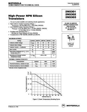
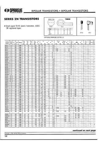
Order this document MOTOROLA by 2N5301/D SEMICONDUCTOR TECHNICAL DATA 2N5301 2N5302 High-Power NPN Silicon 2N5303 Transistors . . . for use in power amplifier and switching circuits applications. 20 AND 30 AMPERE High Collector Emitter Sustaining Voltage POWER TRANSISTORS VCEO(sus) = 80 Vdc (Min) @ IC = 200 mAdc (2N5303) NPN SILICON Low Collector Emitter Saturatio
9.2. Size:56K fairchild semi
2n5308.pdf
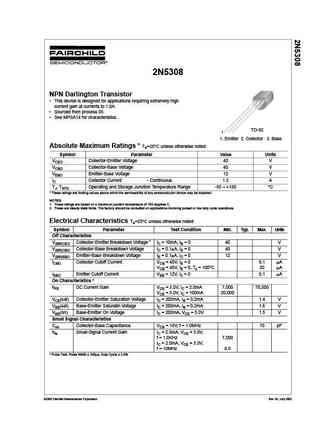
2N5308 NPN Darlington Transistor This device is designed for applications requiring extremely high current gain at currents to 1.0A. Sourced from process 05. See MPSA14 for characteristics. TO-92 1 1. Emitter 2. Collector 3. Base Absolute Maximum Ratings * TA=25 C unless otherwise noted Symbol Parameter Value Units VCEO Collector-Emitter Voltage 40 V VCBO Collector-Bas
9.3. Size:57K fairchild semi
2n5307.pdf
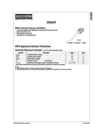
2N5307 NPN General Purpose Amplifier This device designed for applications requiring extremely high current gain at currents to 1.0A. Sourced from Process 05. See MPSA14 for characteristics. TO-92 1 1. Emitter 2. Collector 3. Base NPN Epitaxial Silicon Transistor Absolute Maximum Ratings* Ta=25 C unless otherwise noted Symbol Parameter Value Units VCEO Collector-Emit
9.4. Size:95K central
2n5303.pdf
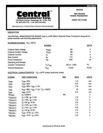
145 Adams Avenue, Hauppauge, NY 11788 USA Tel (631) 435-1110 Fax (631) 435-1824 TM Central Semiconductor Corp. 145 Adams Avenue Hauppauge, NY 11788 USA Tel (631) 435-1110 Fax (631) 435-1824 www.centralsemi.com
9.5. Size:92K onsemi
2n5302.pdf

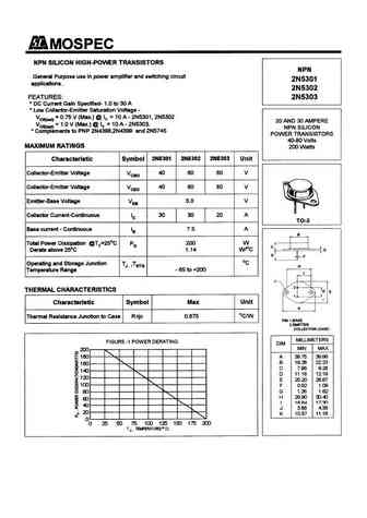
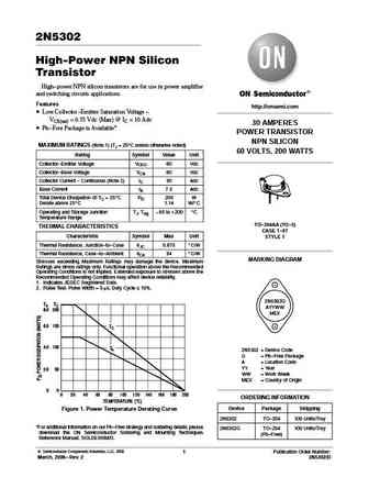
2N5302 High-Power NPN Silicon Transistor High-power NPN silicon transistors are for use in power amplifier and switching circuits applications. Features http //onsemi.com Low Collector-Emitter Saturation Voltage - VCE(sat) = 0.75 Vdc (Max) @ IC = 10 Adc 30 AMPERES Pb-Free Package is Available* POWER TRANSISTOR NPN SILICON MAXIMUM RATINGS (Note 1) (TJ = 25 C unless otherwis
9.6. Size:92K onsemi
2n5302g.pdf
2N5302 High-Power NPN Silicon Transistor High-power NPN silicon transistors are for use in power amplifier and switching circuits applications. Features http //onsemi.com Low Collector-Emitter Saturation Voltage - VCE(sat) = 0.75 Vdc (Max) @ IC = 10 Adc 30 AMPERES Pb-Free Package is Available* POWER TRANSISTOR NPN SILICON MAXIMUM RATINGS (Note 1) (TJ = 25 C unless otherwis
9.10. Size:167K cn sptech
2n5301.pdf
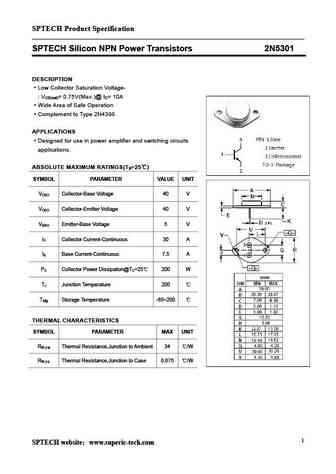
SPTECH Product Specification SPTECH Silicon NPN Power Transistors 2N5301 DESCRIPTION Low Collector Saturation Voltage- V = 0.75V(Max.)@ I = 10A CE(sat) C Wide Area of Safe Operation Complement to Type 2N4398 APPLICATIONS Designed for use in power amplifier and switching circuits applications. ABSOLUTE MAXIMUM RATINGS(T =25 ) a SYMBOL PARAMETER VALUE UNIT V Collector-Ba
9.11. Size:167K cn sptech
2n5302.pdf

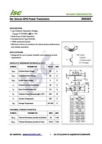
SPTECH Product Specification SPTECH Silicon NPN Power Transistors 2N5302 DESCRIPTION Low Collector Saturation Voltage- V = 0.75V(Max.)@ I = 10A CE(sat) C Wide Area of Safe Operation Complement to Type 2N4399 APPLICATIONS Designed for use in power amplifier and switching circuits applications. ABSOLUTE MAXIMUM RATINGS(T =25 ) a SYMBOL PARAMETER VALUE UNIT V Collector-Ba
9.12. Size:38K inchange semiconductor
2n5301.pdf
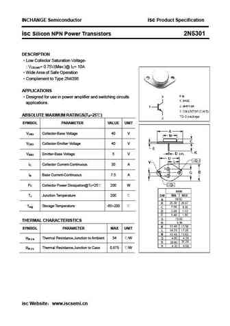
INCHANGE Semiconductor isc Product Specification isc Silicon NPN Power Transistors 2N5301 DESCRIPTION Low Collector Saturation Voltage- VCE(sat)= 0.75V(Max.)@ IC= 10A Wide Area of Safe Operation Complement to Type 2N4398 APPLICATIONS Designed for use in power amplifier and switching circuits applications. ABSOLUTE MAXIMUM RATINGS(Ta=25 ) SYMBOL PARAMETER VALU
9.13. Size:196K inchange semiconductor
2n5302.pdf
INCHANGE Semiconductor isc Silicon NPN Power Transistors 2N5302 DESCRIPTION Low Collector Saturation Voltage- V = 0.75V(Max.)@ I = 10A CE(sat) C Wide Area of Safe Operation Complement to Type 2N4399 100% avalanche tested Minimum Lot-to-Lot variations for robust device performance and reliable operation. APPLICATIONS Designed for use in power amplifier and switching cir
9.14. Size:119K inchange semiconductor
2n5301 2n5302 2n5303.pdf
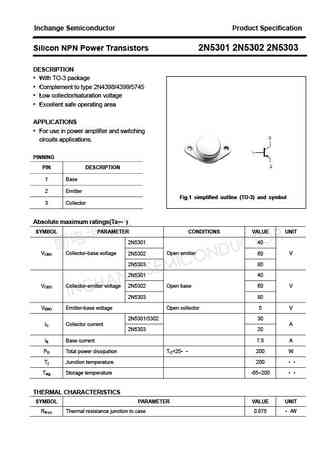
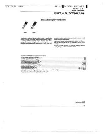
Inchange Semiconductor Product Specification Silicon NPN Power Transistors 2N5301 2N5302 2N5303 DESCRIPTION With TO-3 package Complement to type 2N4398/4399/5745 Low collector/saturation voltage Excellent safe operating area APPLICATIONS For use in power amplifier and switching circuits applications. PINNING PIN DESCRIPTION 1 Base 2 Emitter Fig.1 simplified o
Otros transistores... 2N5298
, 2N53
, 2N530
, 2N5301
, 2N5302
, 2N5303
, 2N5304
, 2N5305
, D882
, 2N5306A
, 2N5307
, 2N5308
, 2N5308A
, 2N5309
, 2N531
, 2N5310
, 2N5311
.