2N5404 Datasheet. Equivalente. Reemplazo. Hoja de especificaciones. Principales características
Número de Parte: 2N5404 📄📄
Material: Si
Polaridad de transistor: PNP
ESPECIFICACIONES MÁXIMAS
Disipación total del dispositivo (Pc): 1 W
Tensión colector-base (Vcb): 80 V
Tensión colector-emisor (Vce): 80 V
Corriente del colector DC máxima (Ic): 5 A
Temperatura operativa máxima (Tj): 200 °C
CARACTERÍSTICAS ELÉCTRICAS
Transición de frecuencia (fT): 40 MHz
Capacitancia de salida (Cc): 150 pF
Ganancia de corriente contínua (hFE): 20
Encapsulados: TO5
📄📄 Copiar
Búsqueda de reemplazo de 2N5404
- Selecciónⓘ de transistores por parámetros
2N5404 datasheet
..1. Size:13K semelab
2n5404 2n5405 2n5406 2n5407.pdf 
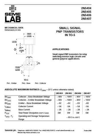
2N5404 2N5405 2N5406 2N5407 MECHANICAL DATA SMALL SIGNAL Dimensions in mm PNP TRANSISTORS 8.89 (0.35) 9.40 (0.37) IN TO-5 7.75 (0.305) 8.51 (0.335) 4.19 (0.165) 4.95 (0.195) 0.89 max. (0.035) 38.1 (1.500) APPLICATIONS min. 7.75 (0.305) 8.51 (0.335) dia. Small signal PNP transistors for relay 5.08 (0.200) switching resistor logic circuits and typ. general purpose appli
9.1. Size:177K motorola
2n5400 2n5401.pdf
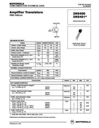
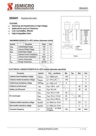
MOTOROLA Order this document SEMICONDUCTOR TECHNICAL DATA by 2N5400/D Amplifier Transistors 2N5400 PNP Silicon * 2N5401 *Motorola Preferred Device COLLECTOR 3 2 BASE 1 EMITTER 1 2 3 MAXIMUM RATINGS Rating Symbol 2N5400 2N5401 Unit CASE 29 04, STYLE 1 TO 92 (TO 226AA) Collector Emitter Voltage VCEO 120 150 Vdc Collector Base Voltage VCBO 130 160 Vdc Emitter B
9.2. Size:52K philips
2n5401.pdf
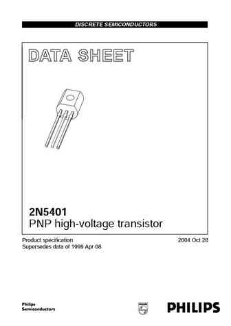
DISCRETE SEMICONDUCTORS DATA SHEET book, halfpage M3D186 2N5401 PNP high-voltage transistor Product specification 2004 Oct 28 Supersedes data of 1999 Apr 08 Philips Semiconductors Product specification PNP high-voltage transistor 2N5401 FEATURES PINNING Low current (max. 300 mA) PIN DESCRIPTION High voltage (max. 150 V). 1 collector 2 base APPLICATIONS 3 emitter G
9.3. Size:432K st
2n5401hr.pdf
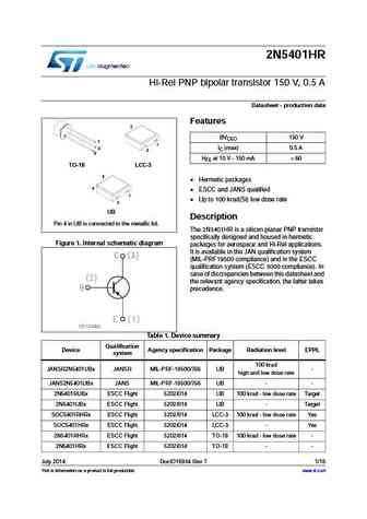
2N5401HR Hi-Rel PNP bipolar transistor 150 V, 0.5 A Datasheet - production data Features 3 BVCEO 150 V 1 1 IC (max) 0.5 A 2 2 3 HFE at 10 V - 150 mA > 60 TO-18 LCC-3 3 Hermetic packages 4 ESCC and JANS qualified 1 Up to 100 krad(Si) low dose rate 2 UB Description Pin 4 in UB is connected to the metallic lid. The 2N5401HR is a silicon planar PNP transistor
9.4. Size:75K fairchild semi
2n5401 mmbt5401.pdf
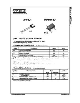
2N5401 MMBT5401 C E C TO-92 B B SOT-23 E Mark 2L PNP General Purpose Amplifier This device is designed as a general purpose amplifier and switch for applications requiring high voltages. Absolute Maximum Ratings* TA = 25 C unless otherwise noted Symbol Parameter Value Units VCEO Collector-Emitter Voltage 150 V VCBO Collector-Base Voltage 160 V VEBO Emitter-Base Voltage 5.0 V I
9.5. Size:546K fairchild semi
2n5400.pdf
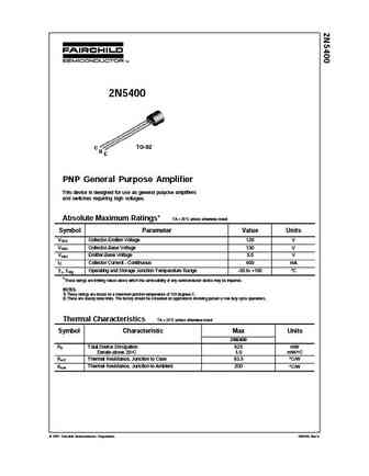
2N5400 C TO-92 B E PNP General Purpose Amplifier This device is designed for use as general purpose amplifiers and switches requiring high voltages. Absolute Maximum Ratings* TA = 25 C unless otherwise noted Symbol Parameter Value Units VCEO Collector-Emitter Voltage 120 V VCBO Collector-Base Voltage 130 V VEBO Emitter-Base Voltage 5.0 V ICCollector Current - Continuous600mA Oper
9.6. Size:53K samsung
2n5401.pdf
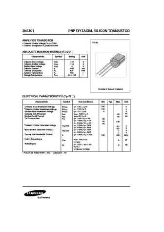
2N5401 PNP EPITAXIAL SILICON TRANSISTOR AMPLIFIER TRANSISTOR TO-92 Collector-Emitter Voltage VCEO= 150V Collector Dissipation PC (max)=625mW ABSOLUTE MAXIMUM RATINGS (T =25 ) A Characteristic Symbol Rating Unit Collector-Base Voltage VCBO -160 V Collector-Emitter Voltage VCEO -150 V Emitter-Base Voltage VEBO -5 V Collector Current IC -600 mA Collector Dissipation PC 625 m
9.7. Size:56K samsung
2n5400.pdf
2N5400 S/S TR CD-ROM(Edition.1.1) This Data Sheet is subject to change without notice. (C) 1994 Samsung Electronics Printed in Korea. Page 1 (2N5400)
9.8. Size:80K central
2n5400 2n5401.pdf
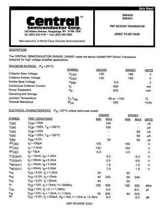
145 Adams Avenue, Hauppauge, NY 11788 USA Tel (631) 435-1110 Fax (631) 435-1824
9.9. Size:275K mcc
2n5401.pdf
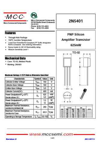
2N5401 MCC TM Micro Commercial Components ELECTRICAL CHARACTERISTICS (TA = 25 C unless otherwise noted) Characteristic Symbol Min Max Unit OFF CHARACTERISTICS Collector Emitter Breakdown Voltage(1) V(BR)CEO Vdc (IC = 1.0 mAdc, IB = 0) 150 Collector Base Breakdown Voltage V(BR)CBO Vdc (IC = 100 mAdc, IE = 0) 160 Emitter Base Breakdown Voltage V(BR)EBO 5.0 Vdc (IE
9.10. Size:121K onsemi
2n5401rlrag.pdf
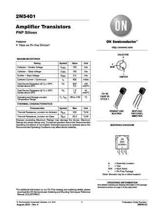
2N5401 Amplifier Transistors PNP Silicon Features These are Pb-Free Devices* http //onsemi.com COLLECTOR 3 MAXIMUM RATINGS Rating Symbol Value Unit 2 BASE Collector - Emitter Voltage VCEO 150 Vdc Collector - Base Voltage VCBO 160 Vdc 1 Emitter - Base Voltage VEBO 5.0 Vdc EMITTER Collector Current - Continuous IC 600 mAdc Total Device Dissipation @ TA = 25 C PD 625 mW Der
9.11. Size:121K onsemi
2n5401g.pdf

2N5401 Amplifier Transistors PNP Silicon Features These are Pb-Free Devices* http //onsemi.com COLLECTOR 3 MAXIMUM RATINGS Rating Symbol Value Unit 2 BASE Collector - Emitter Voltage VCEO 150 Vdc Collector - Base Voltage VCBO 160 Vdc 1 Emitter - Base Voltage VEBO 5.0 Vdc EMITTER Collector Current - Continuous IC 600 mAdc Total Device Dissipation @ TA = 25 C PD 625 mW Der
9.12. Size:145K onsemi
2n5401-d.pdf
2N5401 Amplifier Transistors PNP Silicon Features These are Pb-Free Devices* http //onsemi.com COLLECTOR 3 MAXIMUM RATINGS Rating Symbol Value Unit 2 BASE Collector - Emitter Voltage VCEO 150 Vdc Collector - Base Voltage VCBO 160 Vdc 1 Emitter - Base Voltage VEBO 5.0 Vdc EMITTER Collector Current - Continuous IC 600 mAdc Total Device Dissipation @ TA = 25 C PD 625 mW Der
9.14. Size:253K utc
2n5401.pdf
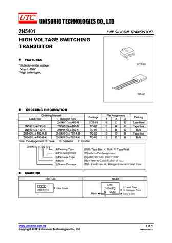
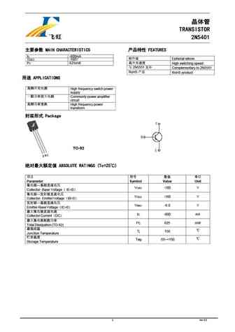
UNISONIC TECHNOLOGIES CO., LTD 2N5401 PNP SILICON TRANSISTOR HIGH VOLTAGE SWITCHING TRANSISTOR FEATURES * Collector-emitter voltage VCEO = -150V * High current gain, ORDERING INFORMATION Ordering Number Pin Assignment Package Packing Lead Free Halogen Free 1 2 3 - 2N5401G-x-AB3-R SOT-89 B C E Tape Reel 2N5401L-x-T92-B 2N5401G-x-T92-B TO-92 E B C Tape Box 2N5401
9.15. Size:250K auk
2n5401.pdf
2N5401 PNP Silicon Transistor Description PIN Connection General purpose amplifier E High voltage application Features B High collector breakdown voltage VCBO = -160V, VCEO = -160V Low collector saturation voltage C VCE(sat)=-0.5V(MAX.) TO-92 Complementary pair with 2N5551 Ordering Information Type NO. Marking Package Code 2N5401 TO-9
9.16. Size:249K auk
2n5401n.pdf
2N5401N Semiconductor Semiconductor PNP Silicon Transistor Description General purpose amplifier High voltage application Features High collector breakdown voltage VCBO = -160V, VCEO = -160V Low collector saturation voltage VCE(sat)=-0.5V(MAX.) Complementary pair with 2N5551N Ordering Information Type NO. Marking Package Code 2N5401N 2N5401 T
9.18. Size:11K semelab
2n5401csm.pdf
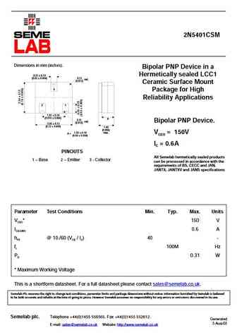
2N5401CSM Dimensions in mm (inches). Bipolar PNP Device in a 0.51 0.10 Hermetically sealed LCC1 (0.02 0.004) 0.31 rad. (0.012) Ceramic Surface Mount 3 Package for High Reliability Applications 21 1.91 0.10 (0.075 0.004) A 0.31 rad. Bipolar PNP Device. (0.012) 3.05 0.13 (0.12 0.005) 1.40 (0.055) 1.02 0.10 max. VCEO = 150V A = (0.04 0.00
9.19. Size:12K semelab
2n5407x.pdf
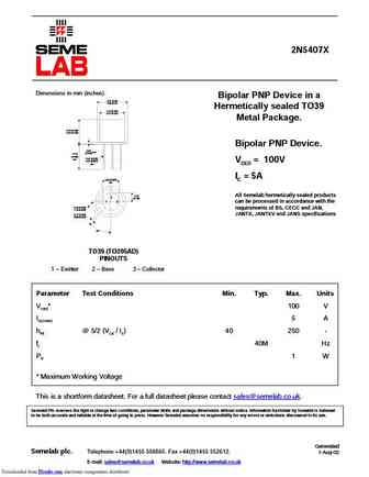
2N5407X Dimensions in mm (inches). Bipolar PNP Device in a 8.51 (0.34) 9.40 (0.37) Hermetically sealed TO39 7.75 (0.305) 8.51 (0.335) Metal Package. 6.10 (0.240) 6.60 (0.260) Bipolar PNP Device. 0.89 (0.035)max. 12.70 (0.500) min. 0.41 (0.016) 0.53 (0.021) VCEO = 100V dia. IC = 5A 5.08 (0.200) typ. 2.54 All Semelab hermetically sealed products 2 (0.100) 1 3
9.20. Size:10K semelab
2n5401dcsm.pdf
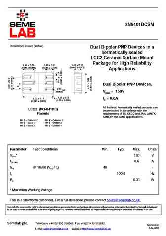
2N5401DCSM Dimensions in mm (inches). Dual Bipolar PNP Devices in a hermetically sealed LCC2 Ceramic Surface Mount Package for High Reliability 1.40 0.15 2.29 0.20 1.65 0.13 (0.055 0.006) (0.09 0.008) (0.065 0.005) Applications 2 3 1 4 Dual Bipolar PNP Devices. A 0.23 6 5 rad. (0.009) V = 150V CEO 6.22 0.13 A = 1.27 0.13 I = 0.6A C (0.
9.21. Size:337K secos
2n5401.pdf
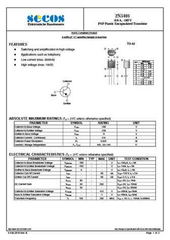
2N5401 -0.6 A, -160 V PNP Plastic Encapsulated Transistor Elektronische Bauelemente RoHS Compliant Product A suffix of -C specifies halogen & lead-free TO-92 FEATURES G H Switching and amplification in high voltage Applications such as telephony J Low current (max. 600mA) A D Millimeter REF. Min. Max. B High voltage (max. 160V) A 4.40 4.70 B 4.30
9.22. Size:375K secos
2n5400.pdf
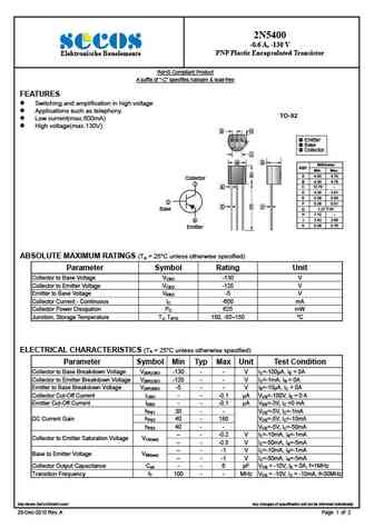
2N5400 -0.6 A, -130 V PNP Plastic Encapsulated Transistor Elektronische Bauelemente RoHS Compliant Product A suffix of -C specifies halogen & lead-free FEATURES Switching and amplification in high voltage Applications such as telephony TO-92 Low current(max.600mA) High voltage(max.130V) G H Emitter Base Collector J A D Millimeter
9.23. Size:274K cdil
2n5401.pdf
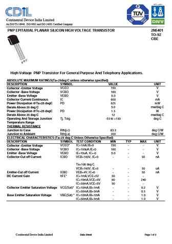
Continental Device India Limited An ISO/TS 16949, ISO 9001 and ISO 14001 Certified Company PNP EPITAXIAL PLANAR SILICON HIGH VOLTAGE TRANSISTOR 2N5401 TO-92 CBE C B E High Voltage PNP Transistor For General Purpose And Telephony Applications. ABSOLUTE MAXIMUM RATINGS(Ta=25deg C unless otherwise specified) DESCRIPTION SYMBOL VALUE UNIT Collector -Emitter Voltage VCEO 150 V Collector
9.24. Size:149K cdil
2n5400.pdf
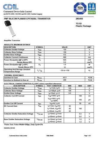
Continental Device India Limited An ISO/TS 16949, ISO 9001 and ISO 14001 Certified Company PNP SILICON PLANAR EPITAXIAL TRANSISTOR 2N5400 TO-92 Plastic Package C B E Amplifier Transistor ABSOLUTE MAXIMUM RATINGS DESCRIPTION SYMBOL VALUE UNIT Collector Emitter Voltage VCEO 120 V Collector Base Voltage VCBO 130 V Emitter Base Voltage VEBO 5.0 V Collector Current Continuous IC 600 mA
9.25. Size:567K jiangsu
2n5401.pdf
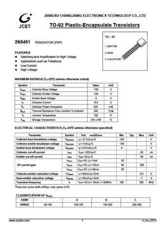
JIANGSU CHANGJIANG ELECTRONICS TECHNOLOGY CO., LTD TO-92 Plastic-Encapsulate Transistors TO 92 2N5401 TRANSISTOR (PNP) 1. EMITTER FEATURES 2. BASE Switching and Amplification in High Voltage 3. COLLECTOR Applications such as Telephony Low Current High Voltage MAXIMUM RATINGS (Ta=25 unless otherwise noted) Symbol Parameter Value Unit VCBO Collector-Base Volta
9.26. Size:355K kec
2n5401.pdf
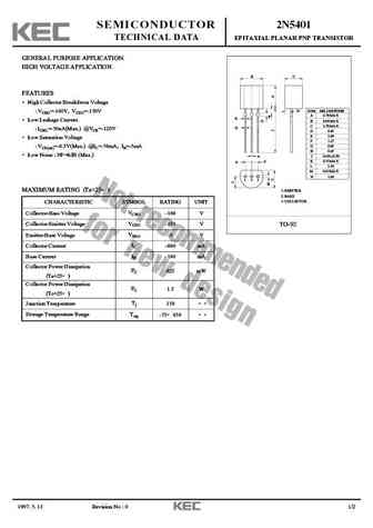
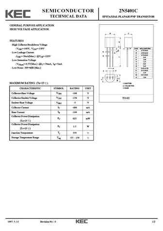
SEMICONDUCTOR 2N5401 TECHNICAL DATA EPITAXIAL PLANAR PNP TRANSISTOR GENERAL PURPOSE APPLICATION. HIGH VOLTAGE APPLICATION. B C FEATURES High Collector Breakdwon Voltage N DIM MILLIMETERS VCBO=-160V, VCEO=-150V A 4.70 MAX E K Low Leakage Current. B 4.80 MAX G C 3.70 MAX D ICBO=-50nA(Max.) @VCB=-120V D 0.45 E 1.00 Low Saturation Voltage F 1.27 G 0.85 VCE(sat)=-
9.27. Size:32K kec
2n5401c.pdf
SEMICONDUCTOR 2N5401C TECHNICAL DATA EPITAXIAL PLANAR PNP TRANSISTOR GENERAL PURPOSE APPLICATION. HIGH VOLTAGE APPLICATION. B C FEATURES High Collector Breakdwon Voltage N DIM MILLIMETERS VCBO=-160V, VCEO=-150V A 4.70 MAX E K Low Leakage Current. B 4.80 MAX G C 3.70 MAX D ICBO=-50nA(Max.) @VCB=-120V D 0.45 E 1.00 Low Saturation Voltage F 1.27 G 0.85 VCE(sat)=-0.5V(
9.28. Size:33K kec
2n5400s.pdf
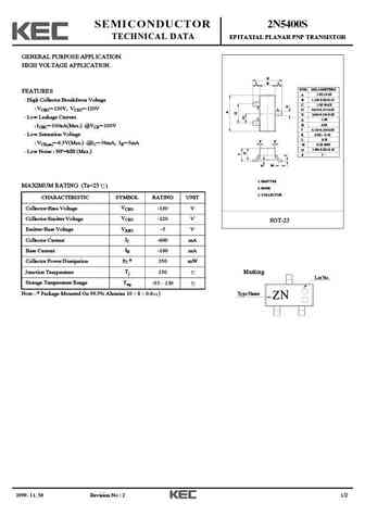
SEMICONDUCTOR 2N5400S TECHNICAL DATA EPITAXIAL PLANAR PNP TRANSISTOR GENERAL PURPOSE APPLICATION. HIGH VOLTAGE APPLICATION. E L B L DIM MILLIMETERS FEATURES _ + 2.93 0.20 A B 1.30+0.20/-0.15 High Collector Breakdwon Voltage C 1.30 MAX 2 VCBO=-130V, VCEO=-120V 3 D 0.45+0.15/-0.05 E 2.40+0.30/-0.20 Low Leakage Current. 1 G 1.90 H 0.95 ICBO=-100nA(Max.) @VCB=-100V J 0.
9.29. Size:32K kec
2n5400.pdf

SEMICONDUCTOR 2N5400 TECHNICAL DATA EPITAXIAL PLANAR PNP TRANSISTOR GENERAL PURPOSE APPLICATION. HIGH VOLTAGE APPLICATION. B C FEATURES High Collector Breakdwon Voltage N DIM MILLIMETERS VCBO=-130V, VCEO=-120V A 4.70 MAX E K Low Leakage Current. B 4.80 MAX G C 3.70 MAX D ICBO=-100nA(Max.) @VCB=-100V D 0.45 E 1.00 Low Saturation Voltage F 1.27 G 0.85 VCE(sat)=-0.5V(
9.30. Size:344K kec
2n5401s.pdf
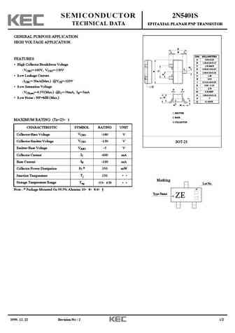
SEMICONDUCTOR 2N5401S TECHNICAL DATA EPITAXIAL PLANAR PNP TRANSISTOR GENERAL PURPOSE APPLICATION. HIGH VOLTAGE APPLICATION. E L B L DIM MILLIMETERS _ FEATURES A 2.93 0.20 + B 1.30+0.20/-0.15 High Collector Breakdwon Voltage C 1.30 MAX 2 3 D 0.40+0.15/-0.05 VCBO=-160V, VCEO=-150V E 2.40+0.30/-0.20 1 Low Leakage Current. G 1.90 H 0.95 ICBO=-50nA(Max.) @VCB=-120V J 0.
9.31. Size:204K lge
2n5401.pdf
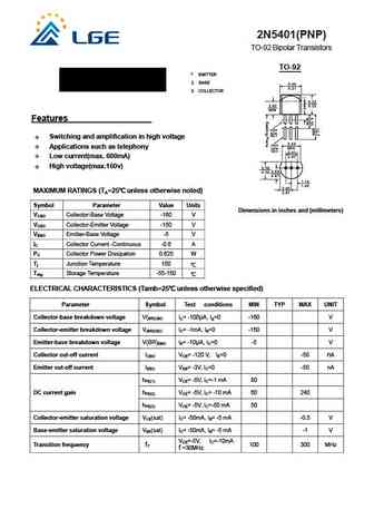
2N5401(PNP) TO-92 Bipolar Transistors TO-92 1. EMITTER 2. BASE 3. COLLECTOR Features Switching and amplification in high voltage Applications such as telephony Low current(max. 600mA) High voltage(max.160v) MAXIMUM RATINGS (TA=25 unless otherwise noted) Symbol Parameter Value Units Dimensions in inches and (millimeters) VCBO Collector-Base Voltage -160 V
9.32. Size:204K lge
2n5400.pdf

2N5400(PNP) TO-92 Bipolar Transistors TO-92 1. EMITTER 2. BASE 3. COLLECTOR Features Switching and amplification in high voltage Applications such as telephony Low current(max. 600mA) High voltage(max.130v) MAXIMUM RATINGS (TA=25 unless otherwise noted) Dimensions in inches and (millimeters) Symbol Parameter Value Units VCBO Collector-Base Voltage -130 V
9.33. Size:680K wietron
2n5401.pdf
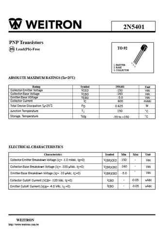
2N5401 PNP Transistors TO-92 1 1. EMITTER 2 3 2. BASE 3. COLLECTOR ABSOLUTE MAXIMUM RATINGS (Ta=25 C) Rating Symbol 2N5401 Unit Collector-Emitter Voltage V CEO -150 Vdc Collector-Base Voltage VCBO -160 Vdc Emitter-Base VOltage VEBO -5.0 Vdc Collector Current IC 600 mAdc Total Device Dissipation T =25 C PD W 0.625 A Junction Temperature T 150 j C Storage, Temperature Tstg
9.34. Size:52K hsmc
h2n5401.pdf
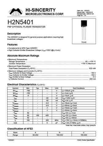
Spec. No. HE6203 HI-SINCERITY Issued Date 1992.09.22 Revised Date 2005.01.20 MICROELECTRONICS CORP. Page No. 1/5 H2N5401 PNP EPITAXIAL PLANAR TRANSISTOR Description The H2N5401 is designed for general purpose applications requiring high breakdown voltages. TO-92 Features Complements to NPN Type H2N5551 High Collector-Emitter Breakdown Voltage (VCEO=150V (@IC=1mA))
9.35. Size:301K shenzhen
2n5401.pdf
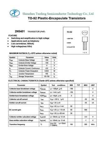
Shenzhen Tuofeng Semiconductor Technology Co., Ltd TO-92 Plastic-Encapsulate Transistors 2N5401 TRANSISTOR (PNP) TO-92 FEATURE Switching and amplification in high voltage 1.EMITTER Applications such as telephony 2.BASE Low current(max. 600mA) High voltage(max.160v) 3.COLLECTOR 1 2 3 MAXIMUM RATINGS (TA=25 unless otherwise noted) Symbol Parameter Value
9.36. Size:307K can-sheng
2n5401.pdf
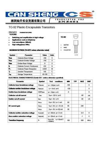
TO-92 Plastic-Encapsulate Transistors TRANSISTOR (PNP) TRANSISTOR (PNP) TRANSISTOR (PNP) 2N5401 TRANSISTOR (PNP) FEATURE FEATURE FEATURE FEATURE TO-92 TO-92 TO-92 TO-92 Switching and amplification in high voltage Switching and amplification in high voltage Switching and amplification in high voltage Switching and amplification in high voltage Applications su
9.37. Size:895K blue-rocket-elect
2n5401.pdf
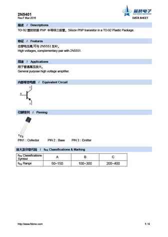
2N5401 Rev.F Mar-2016 DATA SHEET / Descriptions TO-92 PNP Silicon PNP transistor in a TO-92 Plastic Package. / Features , 2N5551 High voltages, complementary pair with 2N5551. / Applications General purpose high voltage amplifier. / Equivalent
9.38. Size:194K semtech
2n5400 2n5401.pdf
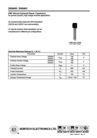
2N5400 / 2N5401 PNP Silicon Epitaxial Planar Transistors for general purpose, high voltage amplifier applications. As complementary types the NPN transistors 2N5550 and 2N5551 are recommended. On special request, these transistors can be manufactured in different pin configurations. 1. Emitter 2. Base 3. Collector TO-92 Plastic Package O Absolute Maximum Ratings (Ta = 25 C)
9.39. Size:170K first silicon
2n5401.pdf
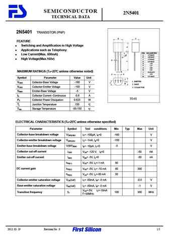
SEMICONDUCTOR 2N5401 TECHNICAL DATA 2N5401 TRANSISTOR (PNP) B C FEATURE Switching and Amplification in High Voltage Applications such as Telephony DIM MILLIMETERS Low Current(Max. 600mA) A 4.70 MAX E B 4.80 MAX G High Voltage(Max.160v) C 3.70 MAX D D 0.55 MAX E 1.00 F 1.27 G 0.85 H 0.45 _ MAXIMUM RATINGS (Ta=25 unless otherwise noted) H J 14.00 0.50 + L 2
9.40. Size:225K first silicon
2n5401s.pdf
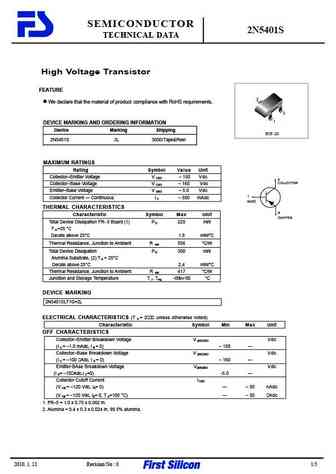
SEMICONDUCTOR 2N5401S TECHNICAL DATA High Voltage Transistor FEATURE 3 We declare that the material of product compliance with RoHS requirements. 2 1 DEVICE MARKING AND ORDERING INFORMATION Device Marking Shipping SOT 23 2N5401S 2L 3000/Tape&Reel MAXIMUM RATINGS Rating Symbol Value Unit Collector Emitter Voltage V 150 Vdc CEO 3 COLLECTOR Collector Base Voltage V CB
9.43. Size:886K slkor
2n5401.pdf
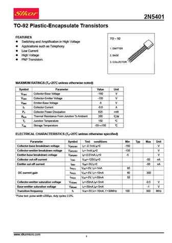
2N5401 TO-92 Plastic-Encapsulate Transistors FEATURES TO 92 Switching and Amplification in High Voltage Applications such as Telephony 1. EMITTER Low Current High Voltage 2. BASE PNP Transistors 3. COLLECTOR MAXIMUM RATINGS (Ta=25 unless otherwise noted) Symbol Parameter Value Unit VCBO Collector-Base Voltage -160 V VCEO Collector-Emitter Voltage -150 V VEB
9.45. Size:565K jsmsemi
2n5401.pdf
2N5401 2N5401 TRANSISTOR (PNP) B C FEATURE Switching and Amplification in High Voltage Applications such as Telephony DIM MILLIMETERS Low Current(Max. 600mA) A 4.70 MAX E B 4.80 MAX G High Voltage(Max.160v) C 3.70 MAX D D 0.55 MAX E 1.00 F 1.27 G 0.85 H 0.45 _ MAXIMUM RATINGS (Ta=25 unless otherwise noted) H J 14.00 0.50 + L 2.30 F F M 0.51 MAX Symbol Pa
9.46. Size:1087K cn cbi
2n5401u.pdf
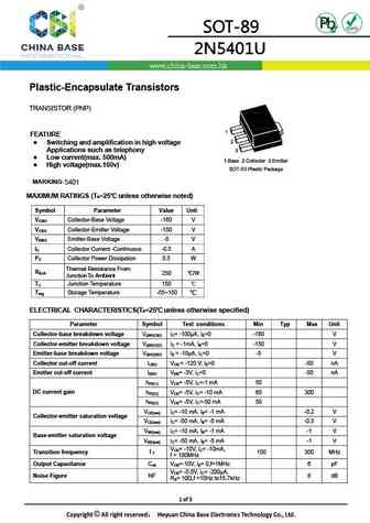
Plastic-Encapsulate Transistors TRANSISTOR (PNP) FEATURE Switching and amplification in high voltage Applications such as telephony Low current(max. 500mA) High voltage(max.160v) MARKING 5401 MAXIMUM RATINGS (Ta=25 unless otherwise noted) Symbol Parameter Value Unit VCBO Collector-Base Voltage -160 V VCEO Collector-Emitter Voltage -150 V VEBO Emitter-Base Volta
Otros transistores... 2N539, 2N5390, 2N5399, 2N539A, 2N54, 2N540, 2N5400, 2N5401, BC558, 2N5405, 2N5406, 2N5407, 2N5408, 2N5409, 2N540A, 2N541, 2N5410