FJD5553 Equivalente. Reemplazo. Hoja de especificaciones. Principales características
Número de Parte: FJD5553
Material: Si
Polaridad de transistor: NPN
ESPECIFICACIONES MÁXIMAS
Disipación total del dispositivo (Pc): 1.25 W
Tensión colector-base (Vcb): 1050 V
Tensión colector-emisor (Vce): 400 V
Tensión emisor-base (Veb): 14 V
Corriente del colector DC máxima (Ic): 3 A
Temperatura operativa máxima (Tj): 150 °C
CARACTERÍSTICAS ELÉCTRICAS
Capacitancia de salida (Cc): 45 pF
Ganancia de corriente contínua (hFE): 30
Encapsulados: TO252
Búsqueda de reemplazo de FJD5553
- Selecciónⓘ de transistores por parámetros
FJD5553 datasheet
fjd5553.pdf
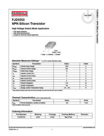
April 2008 FJD5553 NPN Silicon Transistor High Voltage Switch Mode Application Fast Speed Switching Wide Safe Operating Area Suitable for Electronic Ballast Application DPAK 1 Marking J5553 1. Base 2. Collector 3. Emitter Absolute Maximum Ratings * TC=25 C unless otherwise noted Symbol Parameter Value Units BVCBO Collector-Base Voltage 1050 V BVCEO Collector-Emitter
fjd5553.pdf

Is Now Part of To learn more about ON Semiconductor, please visit our website at www.onsemi.com Please note As part of the Fairchild Semiconductor integration, some of the Fairchild orderable part numbers will need to change in order to meet ON Semiconductor s system requirements. Since the ON Semiconductor product management systems do not have the ability to manage part nomenclatur
fjd5553.pdf
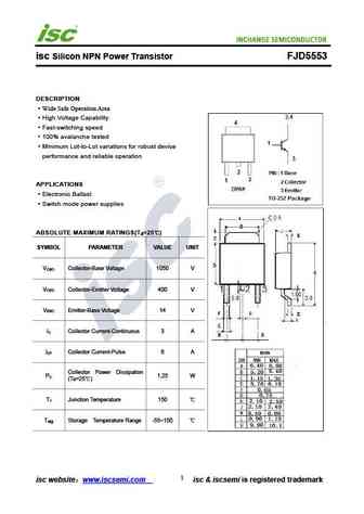
isc Silicon NPN Power Transistor FJD5553 DESCRIPTION Wide Safe Operation Area High Voltage Capability Fast-switching speed 100% avalanche tested Minimum Lot-to-Lot variations for robust device performance and reliable operation APPLICATIONS Electronic Ballast Switch mode power supplies ABSOLUTE MAXIMUM RATINGS(T =25 ) a SYMBOL PARAMETER VALUE UNIT V Collector-Base
fjd5555.pdf
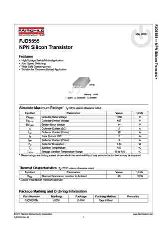
May 2010 FJD5555 NPN Silicon Transistor Features High Voltage Switch Mode Application Fast Speed Switching Wide Safe Operating Area Suitable for Electronic Ballast Application DPAK 1 Marking J5555 1. Base 2. Collector 3. Emitter Absolute Maximum Ratings* Ta=25 C unless otherwise noted Symbol Parameter Value Units BVCBO Collector-Base Voltage 1050 V BVCEO Collec

Otros transistores... FJA4213 , FJA4310 , FJA4313 , FJB102 , FJB3307D , FJD3076 , FJD3305H1 , FJD5304D , 2SD669 , FJD5555 , FJE3303 , FJE5304D , FJI5603D , FJL4215 , FJL4315 , FJL6920 , FJN3303F .
🌐 : EN ES РУ

Liste
Recientemente añadidas las descripciónes de los transistores:
BJT: GA1A4M | SBT42 | 2SA200-Y | 2SA200-O | 2SD882-Q | 2SD882-P | 2SD882-E | 2SC945-L | 2SC945-H | 2SC4226-R23 | 2SC3357-F | 2SC3357-E | 2SC3356-R26 | 2SC3356-R24 | 2SC3356-R23 | 2SB772-Q | 2SB772-P | 2SB772-E | 2SA1015-L | 2SA1015-H | HSS8550
Popular searches
d882 transistor equivalent | 17n80c3 | bc107 transistor | rjp63g4 datasheet | 2sc1115 | c3998 transistor | 2sa679 | 2sc3181