FJD5553 Specs and Replacement
Type Designator: FJD5553
Material of Transistor: Si
Polarity: NPN
Absolute Maximum Ratings
Maximum Collector Power Dissipation (Pc): 1.25 W
Maximum Collector-Base Voltage |Vcb|: 1050 V
Maximum Collector-Emitter Voltage |Vce|: 400 V
Maximum Emitter-Base Voltage |Veb|: 14 V
Maximum Collector Current |Ic max|: 3 A
Max. Operating Junction Temperature (Tj): 150 °C
Electrical Characteristics
Collector Capacitance (Cc): 45 pF
Forward Current Transfer Ratio (hFE), MIN: 30
Package: TO252
FJD5553 Substitution
- BJT ⓘ Cross-Reference Search
FJD5553 datasheet
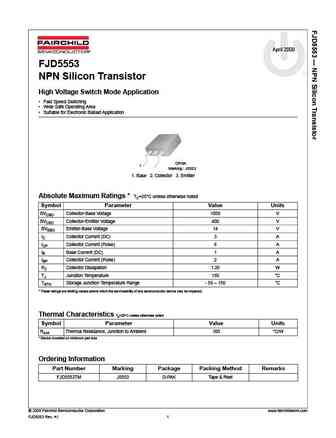
April 2008 FJD5553 NPN Silicon Transistor High Voltage Switch Mode Application Fast Speed Switching Wide Safe Operating Area Suitable for Electronic Ballast Application DPAK 1 Marking J5553 1. Base 2. Collector 3. Emitter Absolute Maximum Ratings * TC=25 C unless otherwise noted Symbol Parameter Value Units BVCBO Collector-Base Voltage 1050 V BVCEO Collector-Emitter... See More ⇒

Is Now Part of To learn more about ON Semiconductor, please visit our website at www.onsemi.com Please note As part of the Fairchild Semiconductor integration, some of the Fairchild orderable part numbers will need to change in order to meet ON Semiconductor s system requirements. Since the ON Semiconductor product management systems do not have the ability to manage part nomenclatur... See More ⇒
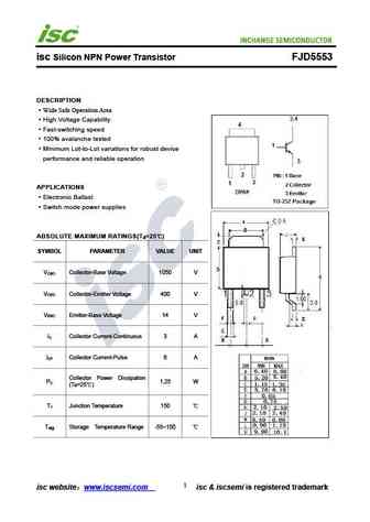
isc Silicon NPN Power Transistor FJD5553 DESCRIPTION Wide Safe Operation Area High Voltage Capability Fast-switching speed 100% avalanche tested Minimum Lot-to-Lot variations for robust device performance and reliable operation APPLICATIONS Electronic Ballast Switch mode power supplies ABSOLUTE MAXIMUM RATINGS(T =25 ) a SYMBOL PARAMETER VALUE UNIT V Collector-Base ... See More ⇒
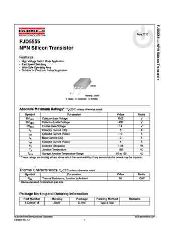
May 2010 FJD5555 NPN Silicon Transistor Features High Voltage Switch Mode Application Fast Speed Switching Wide Safe Operating Area Suitable for Electronic Ballast Application DPAK 1 Marking J5555 1. Base 2. Collector 3. Emitter Absolute Maximum Ratings* Ta=25 C unless otherwise noted Symbol Parameter Value Units BVCBO Collector-Base Voltage 1050 V BVCEO Collec... See More ⇒

Detailed specifications: FJA4213 , FJA4310 , FJA4313 , FJB102 , FJB3307D , FJD3076 , FJD3305H1 , FJD5304D , 2SD669 , FJD5555 , FJE3303 , FJE5304D , FJI5603D , FJL4215 , FJL4315 , FJL6920 , FJN3303F .
Keywords - FJD5553 pdf specs
FJD5553 cross reference
FJD5553 equivalent finder
FJD5553 pdf lookup
FJD5553 substitution
FJD5553 replacement
🌐 : EN ES РУ

LIST
Last Update
BJT: GA1A4M | SBT42 | 2SA200-Y
Popular searches
d882 transistor equivalent | 17n80c3 | bc107 transistor | rjp63g4 datasheet | 2sc1115 | c3998 transistor | 2sa679 | 2sc3181