2N5611 Equivalente. Reemplazo. Hoja de especificaciones. Principales características
Número de Parte: 2N5611
Material: Si
Polaridad de transistor: PNP
ESPECIFICACIONES MÁXIMAS
Disipación total del dispositivo (Pc): 25 W
Tensión colector-base (Vcb): 120 V
Tensión colector-emisor (Vce): 100 V
Tensión emisor-base (Veb): 5 V
Corriente del colector DC máxima (Ic): 5 A
Temperatura operativa máxima (Tj): 200 °C
CARACTERÍSTICAS ELÉCTRICAS
Transición de frecuencia (fT): 560 MHz
Ganancia de corriente contínua (hFE): 30
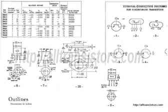
Encapsulados: TO66
Búsqueda de reemplazo de 2N5611
- Selecciónⓘ de transistores por parámetros
2N5611 datasheet
..1. Size:11K semelab
2n5611.pdf 
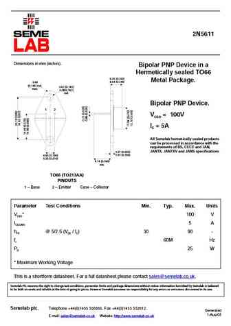
2N5611 Dimensions in mm (inches). Bipolar PNP Device in a Hermetically sealed TO66 6.35 (0.250) Metal Package. 8.64 (0.340) 3.68 (0.145) rad. 3.61 (0.142) max. 4.08(0.161) rad. Bipolar PNP Device. 1 2 VCEO = 100V IC = 5A All Semelab hermetically sealed products can be processed in accordance with the requirements of BS, CECC and JAN, JANTX, JANTXV and JANS speci
..2. Size:126K jmnic
2n5605 2n5607 2n5609 2n5611.pdf
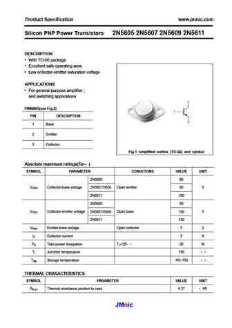
Product Specification www.jmnic.com Silicon PNP Power Transistors 2N5605 2N5607 2N5609 2N5611 DESCRIPTION With TO-66 package Excellent safe operating area Low collector-emitter saturation voltage APPLICATIONS For general-purpose amplifier ; and switching applications PINNING(see Fig.2) PIN DESCRIPTION 1 Base 2 Emitter 3 Collector Fig.1 simplified outline (TO-66)
..3. Size:127K inchange semiconductor
2n5605 2n5607 2n5609 2n5611.pdf
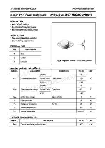
Inchange Semiconductor Product Specification Silicon PNP Power Transistors 2N5605 2N5607 2N5609 2N5611 DESCRIPTION With TO-66 package Excellent safe operating area Low collector saturation voltage APPLICATIONS For general-purpose amplifier ; and switching applications PINNING(see Fig.2) PIN DESCRIPTION 1 Base 2 Emitter Fig.1 simplified outline (TO-66) and symbol
..4. Size:305K inchange semiconductor
2n5611.pdf
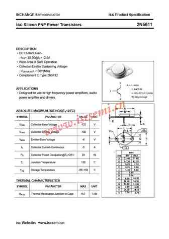
INCHANGE Semiconductor isc Product Specification isc Silicon PNP Power Transistors 2N5611 DESCRIPTION DC Current Gain- hFE= 30-90@IC= -2.5A Wide Area of Safe Operation Collector-Emitter Sustaining Voltage- VCEO(SUS)= -100V(Min) Complement to Type 2N5612 APPLICATIONS Designed for use in high frequency power amplifiers, audio power amplifier and drivers. ABS
0.1. Size:129K inchange semiconductor
2n5611a.pdf
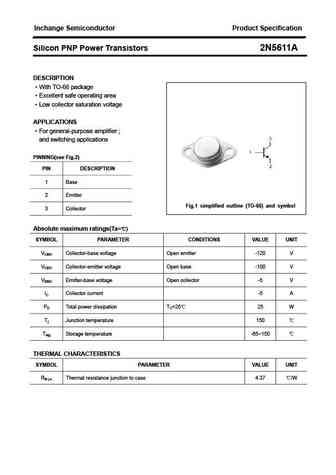
Inchange Semiconductor Product Specification Silicon PNP Power Transistors 2N5611A DESCRIPTION With TO-66 package Excellent safe operating area Low collector saturation voltage APPLICATIONS For general-purpose amplifier ; and switching applications PINNING(see Fig.2) PIN DESCRIPTION 1 Base 2 Emitter Fig.1 simplified outline (TO-66) and symbol 3 Collector Absolu
9.2. Size:11K semelab
2n5613.pdf
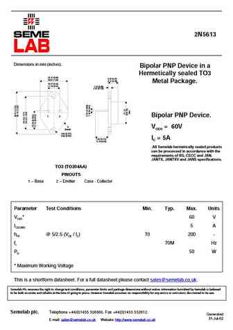
2N5613 Dimensions in mm (inches). Bipolar PNP Device in a Hermetically sealed TO3 25.15 (0.99) 6.35 (0.25) 26.67 (1.05) 9.15 (0.36) Metal Package. 10.67 (0.42) 11.18 (0.44) 1.52 (0.06) 3.43 (0.135) 1 2 Bipolar PNP Device. 3 VCEO = 60V (case) 3.84 (0.151) 4.09 (0.161) 7.92 (0.312) IC = 5A 12.70 (0.50) All Semelab hermetically sealed products can be processed in ac
9.3. Size:11K semelab
2n5619.pdf

2N5619 Dimensions in mm (inches). Bipolar PNP Device in a Hermetically sealed TO3 25.15 (0.99) 6.35 (0.25) 26.67 (1.05) 9.15 (0.36) Metal Package. 10.67 (0.42) 11.18 (0.44) 1.52 (0.06) 3.43 (0.135) 1 2 Bipolar PNP Device. 3 VCEO = 80V (case) 3.84 (0.151) 4.09 (0.161) 7.92 (0.312) IC = 5A 12.70 (0.50) All Semelab hermetically sealed products can be processed in ac
9.4. Size:11K semelab
2n5617.pdf

2N5617 Dimensions in mm (inches). Bipolar PNP Device in a Hermetically sealed TO3 25.15 (0.99) 6.35 (0.25) 26.67 (1.05) 9.15 (0.36) Metal Package. 10.67 (0.42) 11.18 (0.44) 1.52 (0.06) 3.43 (0.135) 1 2 Bipolar PNP Device. 3 VCEO = 80V (case) 3.84 (0.151) 4.09 (0.161) 7.92 (0.312) IC = 5A 12.70 (0.50) All Semelab hermetically sealed products can be processed in ac
9.5. Size:113K jmnic
2n5606 2n5608 2n5610 2n5612.pdf
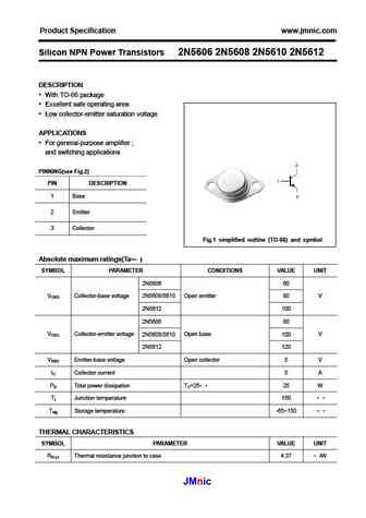
Product Specification www.jmnic.com Silicon NPN Power Transistors 2N5606 2N5608 2N5610 2N5612 DESCRIPTION With TO-66 package Excellent safe operating area Low collector-emitter saturation voltage APPLICATIONS For general-purpose amplifier ; and switching applications PINNING(see Fig.2) PIN DESCRIPTION 1 Base 2 Emitter 3 Collector Fig.1 simplified outline (TO-66)
9.6. Size:127K inchange semiconductor
2n5606 2n5608 2n5610 2n5612.pdf
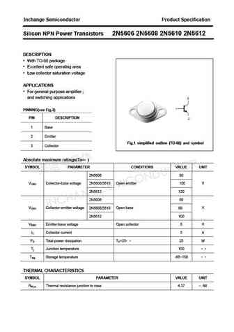
Inchange Semiconductor Product Specification Silicon NPN Power Transistors 2N5606 2N5608 2N5610 2N5612 DESCRIPTION With TO-66 package Excellent safe operating area Low collector saturation voltage APPLICATIONS For general-purpose amplifier ; and switching applications PINNING(see Fig.2) PIN DESCRIPTION 1 Base 2 Emitter Fig.1 simplified outline (TO-66) and symbol
9.7. Size:118K inchange semiconductor
2n5613 2n5615 2n5617 2n5619.pdf
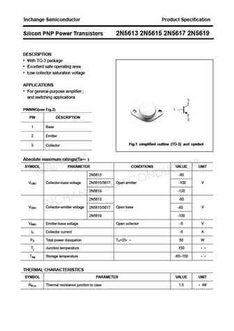
Inchange Semiconductor Product Specification Silicon PNP Power Transistors 2N5613 2N5615 2N5617 2N5619 DESCRIPTION With TO-3 package Excellent safe operating area Low collector saturation voltage APPLICATIONS For general-purpose amplifier ; and switching applications PINNING(see Fig.2) PIN DESCRIPTION 1 Base 2 Emitter Fig.1 simplified outline (TO-3) and symbol
9.8. Size:50K inchange semiconductor
2n5610.pdf
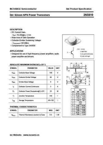
INCHANGE Semiconductor isc Product Specification isc Silicon NPN Power Transistors 2N5610 DESCRIPTION DC Current Gain- hFE= 70-200@IC= 2.5A Wide Area of Safe Operation Collector-Emitter Sustaining Voltage- VCEO(SUS)= 80V(Min) Complement to Type 2N5609 APPLICATIONS Designed for use in high frequency power amplifiers, audio power amplifier and drivers. ABSO
9.9. Size:126K inchange semiconductor
2n5612a.pdf
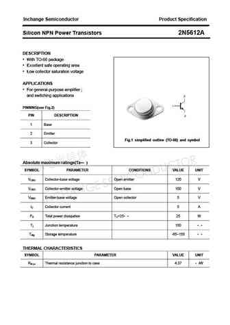
Inchange Semiconductor Product Specification Silicon NPN Power Transistors 2N5612A DESCRIPTION With TO-66 package Excellent safe operating area Low collector saturation voltage APPLICATIONS For general-purpose amplifier ; and switching applications PINNING(see Fig.2) PIN DESCRIPTION 1 Base 2 Emitter Fig.1 simplified outline (TO-66) and symbol 3 Collector Absol
9.10. Size:36K inchange semiconductor
2n5619.pdf
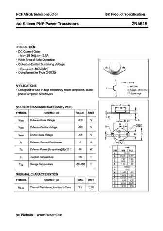
INCHANGE Semiconductor isc Product Specification isc Silicon PNP Power Transistors 2N5619 DESCRIPTION DC Current Gain- hFE= 30-90@IC= -2.5A Wide Area of Safe Operation Collector-Emitter Sustaining Voltage- VCEO(SUS)= -100V(Min) Complement to Type 2N5620 APPLICATIONS Designed for use in high frequency power amplifiers, audio power amplifier and drivers. AB
9.11. Size:118K inchange semiconductor
2n5614 2n5616 2n5618 2n5620.pdf
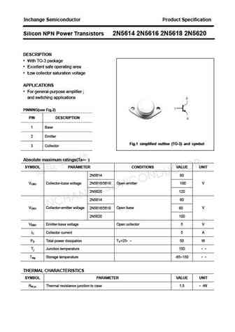
Inchange Semiconductor Product Specification Silicon NPN Power Transistors 2N5614 2N5616 2N5618 2N5620 DESCRIPTION With TO-3 package Excellent safe operating area Low collector saturation voltage APPLICATIONS For general-purpose amplifier ; and switching applications PINNING(see Fig.2) PIN DESCRIPTION 1 Base 2 Emitter Fig.1 simplified outline (TO-3) and symbol 3
Otros transistores... 2N5604
, 2N5605
, 2N5606
, 2N5607
, 2N5608
, 2N5609
, 2N561
, 2N5610
, S8050
, 2N5611A
, 2N5612
, 2N5612A
, 2N5613
, 2N5614
, 2N5615
, 2N5616
, 2N5617
.