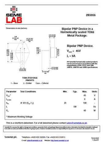
2N5955 Equivalente. Reemplazo. Hoja de especificaciones. Principales características
Número de Parte: 2N5955
Material: Si
Polaridad de transistor: PNP
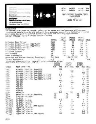
ESPECIFICACIONES MÁXIMAS
Disipación total del dispositivo (Pc): 40 W
Tensión colector-base (Vcb): 70 V
Tensión colector-emisor (Vce): 60 V
Tensión emisor-base (Veb): 5 V
Corriente del colector DC máxima (Ic): 6 A
Temperatura operativa máxima (Tj): 200 °C
CARACTERÍSTICAS ELÉCTRICAS
Transición de frecuencia (ft): 5 MHz
Ganancia de corriente contínua (hfe): 20
Paquete / Cubierta: TO66
Búsqueda de reemplazo de 2N5955
2N5955 PDF detailed specifications
2n5954 2n5955 2n5956 2n6372 2n6373 2n6374.pdf
TM Central Semiconductor Corp. 145 Adams Avenue Hauppauge, NY 11788 USA Tel (631) 435-1110 Fax (631) 435-1824 www.centralsemi.com ... See More ⇒
2n5954 2n5955 2n5956.pdf
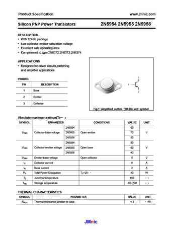
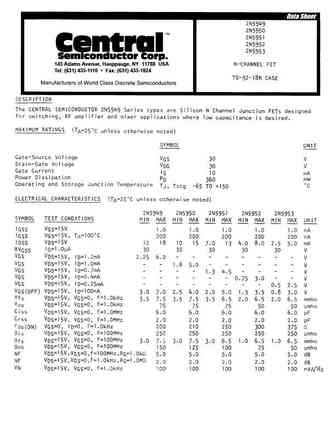
Product Specification www.jmnic.com Silicon PNP Power Transistors 2N5954 2N5955 2N5956 DESCRIPTION With TO-66 package Low collector-emitter saturation voltage Excellent safe operating area Complement to type 2N6372 2N6373 2N6374 APPLICATIONS Designed for driver circuits,switching and amplifier applications PINNING PIN DESCRIPTION 1 Base 2 Emitter 3 Collector ... See More ⇒
2n5954 2n5955 2n5956.pdf
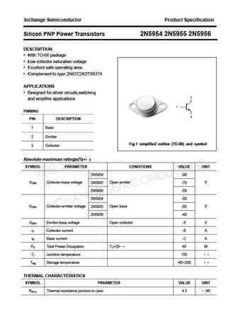
Inchange Semiconductor Product Specification Silicon PNP Power Transistors 2N5954 2N5955 2N5956 DESCRIPTION With TO-66 package Low collector saturation voltage Excellent safe operating area Complement to type 2N6372/6373/6374 APPLICATIONS Designed for driver circuits,switching and amplifier applications PINNING PIN DESCRIPTION 1 Base 2 Emitter Fig.1 simplifie... See More ⇒
2n5951.pdf

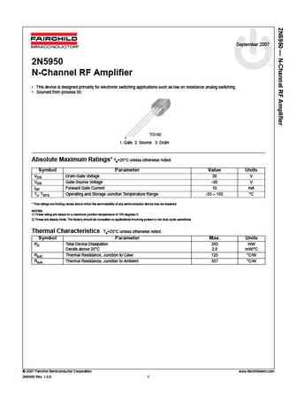
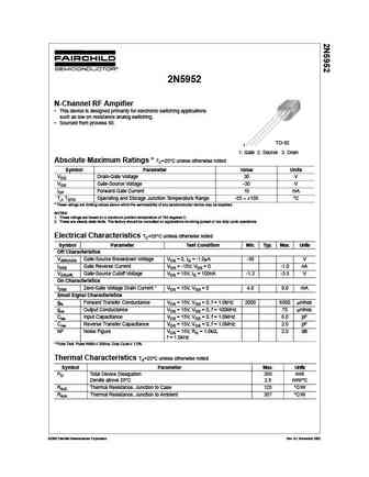
September 2007 2N5951 N-Channel RF Amplifier This device is designed primarily for electronic switching applications such as low on resistance analog switching. Sourced from process 50. TO-92 1 1. Gate 2. Source 3. Drain Absolute Maximum Ratings* Ta=25 C unless otherwise noted Symbol Parameter Value Units VDG Drain-Gate Voltage 30 V VGS Gate-Source Voltage -30 V IGF Forward... See More ⇒
Otros transistores... 2N5942 , 2N5943 , 2N5944 , 2N5945 , 2N5946 , 2N5947 , 2N595 , 2N5954 , B772 , 2N5956 , 2N5957 , 2N5958 , 2N5959 , 2N596 , 2N5960 , 2N5961 , 2N5962 .


Liste
Recientemente añadidas las descripciónes de los transistores:
BJT: GA1A4M | SBT42 | 2SA200-Y | 2SA200-O | 2SD882-Q | 2SD882-P | 2SD882-E | 2SC945-L | 2SC945-H | 2SC4226-R23 | 2SC3357-F | 2SC3357-E | 2SC3356-R26 | 2SC3356-R24 | 2SC3356-R23 | 2SB772-Q | 2SB772-P | 2SB772-E | 2SA1015-L | 2SA1015-H | HSS8550
Popular searches
hy3210 | d313 transistor equivalent | 2sb827 | c5200 datasheet | 2n2614 | 2sa777 replacement | 2sc828 transistor | 2sd357