2N62 Equivalente. Reemplazo. Hoja de especificaciones. Principales características
Número de Parte: 2N62
Material: Ge
Polaridad de transistor: PNP
ESPECIFICACIONES MÁXIMAS
Disipación total del dispositivo (Pc): 0.05 W
Tensión colector-base (Vcb): 35 V
Corriente del colector DC máxima (Ic): 0.02 A
Temperatura operativa máxima (Tj): 85 °C
CARACTERÍSTICAS ELÉCTRICAS
Ganancia de corriente contínua (hFE): 25
Encapsulados: TO23
Búsqueda de reemplazo de 2N62
- Selecciónⓘ de transistores por parámetros
2N62 datasheet
2n6282 2n6283 2n6284 2n6285 2n6286 2n6287.pdf
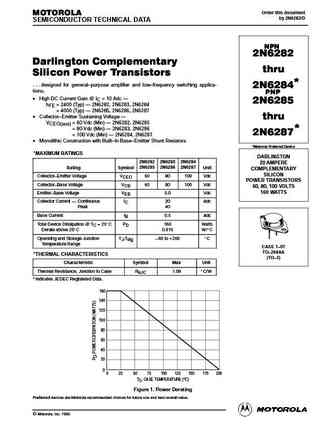
Order this document MOTOROLA by 2N6282/D SEMICONDUCTOR TECHNICAL DATA NPN 2N6282 Darlington Complementary thru Silicon Power Transistors . . . designed for general purpose amplifier and low frequency switching applica- 2N6284* tions. PNP High DC Current Gain @ IC = 10 Adc 2N6285 hFE = 2400 (Typ) 2N6282, 2N6283, 2N6284 hFE = 4000 (Typ) 2N6285, 2N6286, 2N6287
2n6251re.pdf
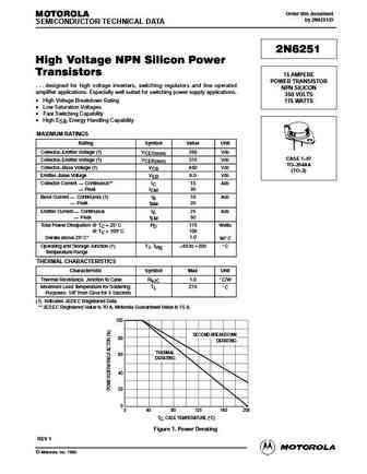
Order this document MOTOROLA by 2N6251/D SEMICONDUCTOR TECHNICAL DATA 2N6251 High Voltage NPN Silicon Power Transistors 15 AMPERE POWER TRANSISTOR . . . designed for high voltage inverters, switching regulators and line operated NPN SILICON amplifier applications. Especially well suited for switching power supply applications. 350 VOLTS High Voltage Breakdown Rating 175 WATTS
2n6107 2n6111 2n6288 2n6109 2n6292.pdf
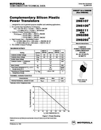
Order this document MOTOROLA by 2N6107/D SEMICONDUCTOR TECHNICAL DATA 2N6057 thru 2N6059 (See 2N6050) Complementary Silicon Plastic PNP Power Transistors 2N6107 . . . designed for use in general purpose amplifier and switching applications. 2N6109* DC Current Gain Specified to 7.0 Amperes hFE = 30 150 @ IC = 3.0 Adc 2N6111, 2N6288 hFE = 2.3 (Min) @ IC = 7.0 Adc All
2n6274-75 2n6277 2n6274 2n6275 2n6277.pdf
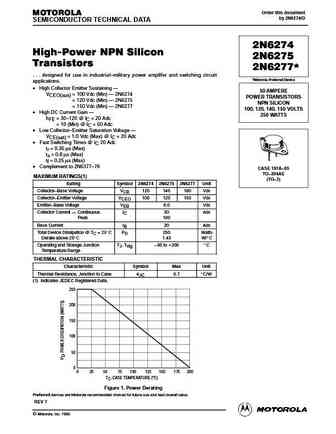
Order this document MOTOROLA by 2N6274/D SEMICONDUCTOR TECHNICAL DATA 2N6274 High-Power NPN Silicon 2N6275 Transistors 2N6277 * . . . designed for use in industrial military power amplifer and switching circuit *Motorola Preferred Device applications. High Collector Emitter Sustaining 50 AMPERE VCEO(sus) = 100 Vdc (Min) 2N6274 POWER TRANSISTORS VCEO(sus) = 120 Vdc
2n6237 2n6238 2n6239 2n6240 2n6241.pdf
MOTOROLA Order this document SEMICONDUCTOR TECHNICAL DATA by 2N6237/D 2N6237 thru Silicon Controlled Rectifiers 2N6241 Reverse Blocking Triode Thyristors . . . PNPN devices designed for high volume consumer applications such as SCRs temperature, light, and speed control; process and remote control, and warning 4 AMPERES RMS systems where reliability of operation is important. 50 t
std2n62k3 stf2n62k3 stu2n62k3.pdf
STD2N62K3, STF2N62K3, STU2N62K3 Datasheet N-channel 620 V, 2.9 typ., 2.2 A MDmesh K3 Power MOSFETs in DPAK, TO-220FP and IPAK packages Features VDS RDS(on)max. ID Order code Package STD2N62K3 DPAK STF2N62K3 620 V 3.6 2.2 A TO-220FP STU2N62K3 IPAK D(2, TAB) 100% avalanche tested Extremely high dv/dt capability Very low intrinsic capacitance G(1) Improved
stb2n62k3.pdf

STB2N62K3, STD2N62K3, STF2N62K3, STP2N62K3, STU2N62K3 N-channel 620 V, 3 , 2.2 A SuperMESH3 Power MOSFET in D PAK, DPAK, TO-220FP, TO-220 and IPAK packages Datasheet production data Features TAB RDS(on) Order codes VDSS max ID PTOT 3 2 3 1 1 STB2N62K3 TAB 45 W IPAK D PAK STD2N62K3 3 TAB STF2N62K3 620 V
stb2n62k3 std2n62k3 stf2n62k3 stp2n62k3 stu2n62k3.pdf
STB2N62K3, STD2N62K3, STF2N62K3, STP2N62K3, STU2N62K3 N-channel 620 V, 3 , 2.2 A SuperMESH3 Power MOSFET in D PAK, DPAK, TO-220FP, TO-220 and IPAK packages Datasheet production data Features TAB RDS(on) Order codes VDSS max ID PTOT 3 2 3 1 1 STB2N62K3 TAB 45 W IPAK D PAK STD2N62K3 3 TAB STF2N62K3 620 V
std2n62k3 stf2n62k3 stu2n62k3 stp2n62k3.pdf
STD2N62K3, STF2N62K3 STP2N62K3, STU2N62K3 N-channel 620 V, 3 , 2.2 A, DPAK, IPAK, TO-220, TO-220FP SuperMESH3 Power MOSFET Features RDS(on) 3 Type VDSS ID Pw max 1 3 2 DPAK 1 STD2N62K3 45 W IPAK STF2N62K3 20 W 620 V
2n6284 2n6287.pdf
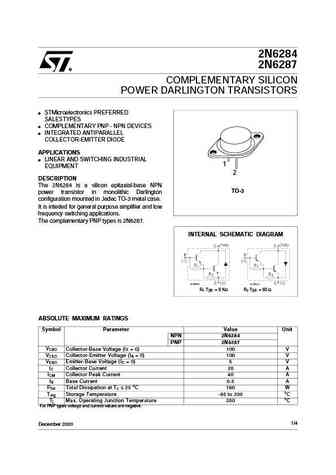
2N6284 2N6287 COMPLEMENTARY SILICON POWER DARLINGTON TRANSISTORS STMicroelectronics PREFERRED SALESTYPES COMPLEMENTARY PNP - NPN DEVICES INTEGRATED ANTIPARALLEL COLLECTOR-EMITTER DIODE APPLICATIONS LINEAR AND SWITCHING INDUSTRIAL 1 EQUIPMENT 2 DESCRIPTION The 2N6284 is a silicon epitaxial-base NPN TO-3 power transistor in monolithic Darlington configuration moun
2n6294 2n6295 2n6296 2n6297.pdf
145 Adams Avenue, Hauppauge, NY 11788 USA Tel (631) 435-1110 Fax (631) 435-1824
2n6249 2n6250 2n6251.pdf
145 Adams Avenue, Hauppauge, NY 11788 USA Tel (631) 435-1110 Fax (631) 435-1824 TM Central Semiconductor Corp. 145 Adams Avenue Hauppauge, NY 11788 USA Tel (631) 435-1110 Fax (631) 435-1824 www.centralsemi.com
2n6107 2n6109 2n6111 2n6288 2n6290 2n6292.pdf
145 Adams Avenue, Hauppauge, NY 11788 USA Tel (631) 435-1110 Fax (631) 435-1824
2n6284g 2n6284g 2n6287g.pdf

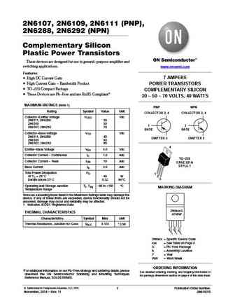
2N6284 (NPN); 2N6286, 2N6287 (PNP) Preferred Device Darlington Complementary Silicon Power Transistors These packages are designed for general-purpose amplifier and low-frequency switching applications. http //onsemi.com Features 20 AMPERE High DC Current Gain @ IC = 10 Adc - COMPLEMENTARY SILICON hFE = 2400 (Typ) - 2N6284 POWER TRANSISTORS = 4000 (Typ) - 2N6287 100 VOLTS, 1
2n6107g 2n6109g 2n6111g 2n6288g 2n6292g.pdf

2N6107, 2N6109, 2N6111 (PNP), 2N6288, 2N6292 (NPN) Complementary Silicon Plastic Power Transistors These devices are designed for use in general-purpose amplifier and switching applications. www.onsemi.com Features 7 AMPERE High DC Current Gain High Current Gain - Bandwidth Product POWER TRANSISTORS TO-220 Compact Package COMPLEMENTARY SILICON These Devices are Pb-
2n6107 2n6109 2n6111 2n6288 2n6292.pdf
2N6107, 2N6109, 2N6111 (PNP), 2N6288, 2N6292 (NPN) Complementary Silicon Plastic Power Transistors These devices are designed for use in general-purpose amplifier and switching applications. www.onsemi.com Features 7 AMPERE High DC Current Gain High Current Gain - Bandwidth Product POWER TRANSISTORS TO-220 Compact Package COMPLEMENTARY SILICON These Devices are Pb-
2n6288g.pdf
PNP - 2N6107, 2N6109, 2N6111; NPN - 2N6288, 2N6292 Complementary Silicon Plastic Power Transistors http //onsemi.com These devices are designed for use in general-purpose amplifier and switching applications. 7 AMPERE Features POWER TRANSISTORS DC Current Gain Specified to 7.0 Amperes hFE = 30-150 @ IC COMPLEMENTARY SILICON = 3.0 Adc - 2N6111, 2N6288 30 - 50 - 70 VOLTS, 40 WA
2n6292g.pdf

2N6107, 2N6109, 2N6111 (PNP), 2N6288, 2N6292 (NPN) Complementary Silicon Plastic Power Transistors These devices are designed for use in general-purpose amplifier and switching applications. www.onsemi.com Features 7 AMPERE High DC Current Gain High Current Gain - Bandwidth Product POWER TRANSISTORS TO-220 Compact Package COMPLEMENTARY SILICON These Devices are Pb-
2n6287g.pdf

2N6284 (NPN); 2N6286, 2N6287 (PNP) Preferred Device Darlington Complementary Silicon Power Transistors These packages are designed for general-purpose amplifier and low-frequency switching applications. http //onsemi.com Features 20 AMPERE High DC Current Gain @ IC = 10 Adc - COMPLEMENTARY SILICON hFE = 2400 (Typ) - 2N6284 POWER TRANSISTORS = 4000 (Typ) - 2N6287 100 VOLTS, 1
2n6111g 2n6111g 2n6292g.pdf

2N6107, 2N6109, 2N6111 (PNP), 2N6288, 2N6292 (NPN) Complementary Silicon Plastic Power Transistors These devices are designed for use in general-purpose amplifier and switching applications. www.onsemi.com Features 7 AMPERE High DC Current Gain High Current Gain - Bandwidth Product POWER TRANSISTORS TO-220 Compact Package COMPLEMENTARY SILICON These Devices are Pb-
2n6286g.pdf
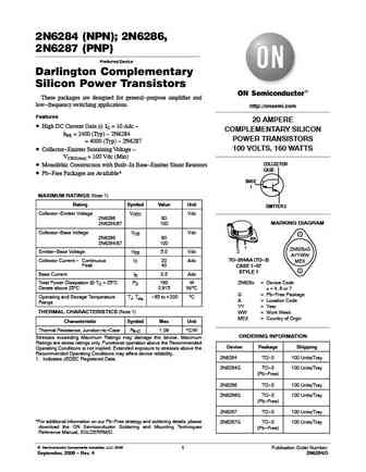
2N6284 (NPN); 2N6286, 2N6287 (PNP) Preferred Device Darlington Complementary Silicon Power Transistors These packages are designed for general-purpose amplifier and low-frequency switching applications. http //onsemi.com Features 20 AMPERE High DC Current Gain @ IC = 10 Adc - COMPLEMENTARY SILICON hFE = 2400 (Typ) - 2N6284 POWER TRANSISTORS = 4000 (Typ) - 2N6287 100 VOLTS, 1
2n6249-2n6250-2n6251.pdf
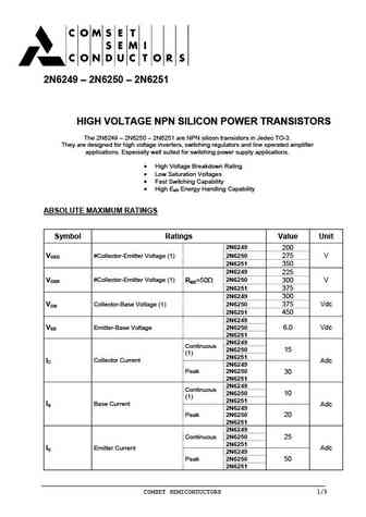
2N6249 2N6250 2N6251 HIGH VOLTAGE NPN SILICON POWER TRANSISTORS HIGH VOLTAGE NPN SILICON POWER TRANSISTORS The 2N6249 2N6250 2N6251 are NPN silicon transistors in Jedec TO-3. They are designed for high voltage inverters, switching regulators and line operated amplifier applications. Especially well suited for switching power supply applications. High Voltage Breakdown
2n6253-2n6254-2n6371.pdf
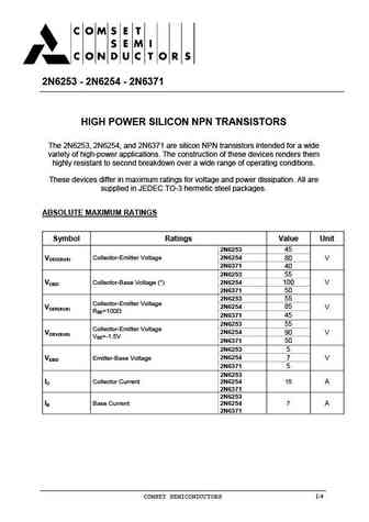
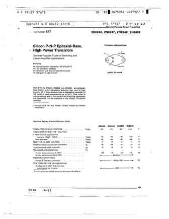
2N6253 - 2N6254 - 2N6371 HIGH POWER SILICON NPN TRANSISTORS The 2N6253, 2N6254, and 2N6371 are silicon NPN transistors intended for a wide variety of high-power applications. The construction of these devices renders them highly resistant to second breakdown over a wide range of operating conditions. These devices differ in maximum ratings for voltage and power dissipation. All are suppli
2n6247.pdf

2N6247 Dimensions in mm (inches). Bipolar PNP Device in a Hermetically sealed TO3 25.15 (0.99) 6.35 (0.25) 26.67 (1.05) 9.15 (0.36) Metal Package. 10.67 (0.42) 11.18 (0.44) 1.52 (0.06) 3.43 (0.135) 1 2 Bipolar PNP Device. 3 VCEO = 90V (case) 3.84 (0.151) 4.09 (0.161) 7.92 (0.312) IC = 10A 12.70 (0.50) All Semelab hermetically sealed products can be processed in a
2n6254.pdf

2N6254 Dimensions in mm (inches). Bipolar NPN Device in a Hermetically sealed TO3 25.15 (0.99) 6.35 (0.25) 26.67 (1.05) 9.15 (0.36) Metal Package. 10.67 (0.42) 11.18 (0.44) 1.52 (0.06) 3.43 (0.135) 1 2 Bipolar NPN Device. 3 VCEO = 80V (case) 3.84 (0.151) 4.09 (0.161) 7.92 (0.312) IC = 15A 12.70 (0.50) All Semelab hermetically sealed products can be processed in a
2n6245.pdf
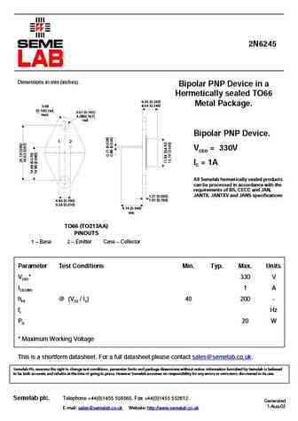
2N6245 Dimensions in mm (inches). Bipolar PNP Device in a Hermetically sealed TO66 6.35 (0.250) Metal Package. 8.64 (0.340) 3.68 (0.145) rad. 3.61 (0.142) max. 4.08(0.161) rad. Bipolar PNP Device. 1 2 VCEO = 330V IC = 1A All Semelab hermetically sealed products can be processed in accordance with the requirements of BS, CECC and JAN, JANTX, JANTXV and JANS speci
2n6246.pdf

2N6246 Dimensions in mm (inches). Bipolar PNP Device in a Hermetically sealed TO3 25.15 (0.99) 6.35 (0.25) 26.67 (1.05) 9.15 (0.36) Metal Package. 10.67 (0.42) 11.18 (0.44) 1.52 (0.06) 3.43 (0.135) 1 2 Bipolar PNP Device. 3 VCEO = 70V (case) 3.84 (0.151) 4.09 (0.161) 7.92 (0.312) IC = 10A 12.70 (0.50) All Semelab hermetically sealed products can be processed in a
2n6230.pdf

2N6230 Dimensions in mm (inches). Bipolar PNP Device in a Hermetically sealed TO3 25.15 (0.99) 6.35 (0.25) 26.67 (1.05) 9.15 (0.36) Metal Package. 10.67 (0.42) 11.18 (0.44) 1.52 (0.06) 3.43 (0.135) 1 2 Bipolar PNP Device. 3 VCEO = 120V (case) 3.84 (0.151) 4.09 (0.161) 7.92 (0.312) IC = 10A 12.70 (0.50) All Semelab hermetically sealed products can be processed in
2n6262.pdf
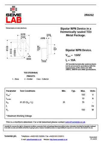
2N6262 Dimensions in mm (inches). Bipolar NPN Device in a Hermetically sealed TO3 25.15 (0.99) 6.35 (0.25) 26.67 (1.05) 9.15 (0.36) Metal Package. 10.67 (0.42) 11.18 (0.44) 1.52 (0.06) 3.43 (0.135) 1 2 Bipolar NPN Device. 3 VCEO = 150V (case) 3.84 (0.151) 4.09 (0.161) 7.92 (0.312) IC = 10A 12.70 (0.50) All Semelab hermetically sealed products can be processed in
2n6235x.pdf
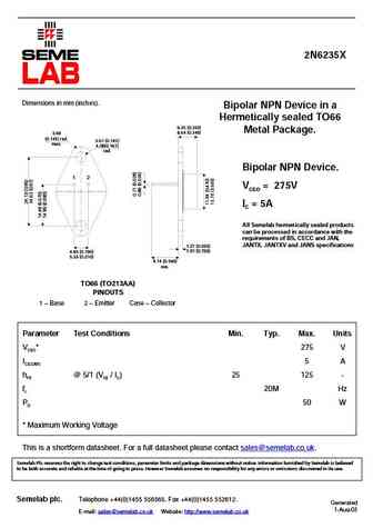
2N6235X Dimensions in mm (inches). Bipolar NPN Device in a Hermetically sealed TO66 6.35 (0.250) Metal Package. 8.64 (0.340) 3.68 (0.145) rad. 3.61 (0.142) max. 4.08(0.161) rad. Bipolar NPN Device. 1 2 VCEO = 275V IC = 5A All Semelab hermetically sealed products can be processed in accordance with the requirements of BS, CECC and JAN, JANTX, JANTXV and JANS spec
2n6226.pdf

2N6226 Dimensions in mm (inches). Bipolar PNP Device in a Hermetically sealed TO3 25.15 (0.99) 6.35 (0.25) 26.67 (1.05) 9.15 (0.36) Metal Package. 10.67 (0.42) 11.18 (0.44) 1.52 (0.06) 3.43 (0.135) 1 2 Bipolar PNP Device. 3 VCEO = 100V (case) 3.84 (0.151) 4.09 (0.161) 7.92 (0.312) IC = 6A 12.70 (0.50) All Semelab hermetically sealed products can be processed in a
2n6263.pdf
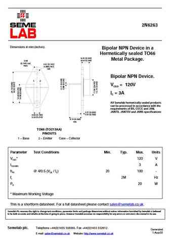
2N6263 Dimensions in mm (inches). Bipolar NPN Device in a Hermetically sealed TO66 6.35 (0.250) Metal Package. 8.64 (0.340) 3.68 (0.145) rad. 3.61 (0.142) max. 4.08(0.161) rad. Bipolar NPN Device. 1 2 VCEO = 120V IC = 3A All Semelab hermetically sealed products can be processed in accordance with the requirements of BS, CECC and JAN, JANTX, JANTXV and JANS speci
2n6299smd05 2n6299smd 2n6301smd 2n6301smd05.pdf
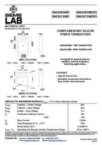
2N6299SMD 2N6299SMD05 2N6301SMD 2N6301SMD05 MECHANICAL DATA Dimensions in mm (inches) COMPLEMENTARY SILICON POWER TRANSISTORS 2N6299SMD - PNP TRANSISTOR 2N6301SMD - NPN TRANSISTOR Designed for general
2n6261.pdf
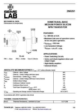
2N6261 MECHANICAL DATA HOMETAXIAL-BASE Dimensions in mm(inches) MEDIUM POWER SILICON NPN TRANSISTOR 6.35 (0.250) 8.64 (0.340) 3.68 (0.145) rad. 3.61 (0.142) max. 3.86 (0.145) rad. FEATURES fT = 800 kHz at 0.2A Maximum Safe-area of operation curves for dc and pulse operation. VCEV(sus) = 90V min Low Saturation Voltage VCE(sat = 1.0V at IC = 0.5A) 1.27 (0.050
2n6235.pdf
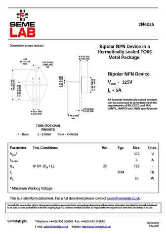
2N6235 Dimensions in mm (inches). Bipolar NPN Device in a Hermetically sealed TO66 6.35 (0.250) Metal Package. 8.64 (0.340) 3.68 (0.145) rad. 3.61 (0.142) max. 4.08(0.161) rad. Bipolar NPN Device. 1 2 VCEO = 325V IC = 5A All Semelab hermetically sealed products can be processed in accordance with the requirements of BS, CECC and JAN, JANTX, JANTXV and JANS speci
2n6234.pdf

2N6234 Dimensions in mm (inches). Bipolar NPN Device in a Hermetically sealed TO66 6.35 (0.250) Metal Package. 8.64 (0.340) 3.68 (0.145) rad. 3.61 (0.142) max. 4.08(0.161) rad. Bipolar NPN Device. 1 2 VCEO = 275V IC = 5A All Semelab hermetically sealed products can be processed in accordance with the requirements of BS, CECC and JAN, JANTX, JANTXV and JANS speci
2n6253.pdf

2N6253 Dimensions in mm (inches). Bipolar NPN Device in a Hermetically sealed TO3 25.15 (0.99) 6.35 (0.25) 26.67 (1.05) 9.15 (0.36) Metal Package. 10.67 (0.42) 11.18 (0.44) 1.52 (0.06) 3.43 (0.135) 1 2 Bipolar NPN Device. 3 VCEO = 45V (case) 3.84 (0.151) 4.09 (0.161) 7.92 (0.312) IC = 15A 12.70 (0.50) All Semelab hermetically sealed products can be processed in a
2n6260.pdf
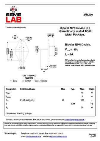
2N6260 Dimensions in mm (inches). Bipolar NPN Device in a Hermetically sealed TO66 6.35 (0.250) Metal Package. 8.64 (0.340) 3.68 (0.145) rad. 3.61 (0.142) max. 4.08(0.161) rad. Bipolar NPN Device. 1 2 VCEO = 40V IC = 3A All Semelab hermetically sealed products can be processed in accordance with the requirements of BS, CECC and JAN, JANTX, JANTXV and JANS specif
2n6270.pdf

2N6270 Dimensions in mm (inches). Bipolar NPN Device in a Hermetically sealed TO3 25.15 (0.99) 6.35 (0.25) 26.67 (1.05) 9.15 (0.36) Metal Package. 10.67 (0.42) 11.18 (0.44) 1.52 (0.06) 3.43 (0.135) 1 2 Bipolar NPN Device. 3 VCEO = 80V (case) 3.84 (0.151) 4.09 (0.161) 7.92 (0.312) IC = 30A 12.70 (0.50) All Semelab hermetically sealed products can be processed in a
2n6227.pdf

2N6227 Dimensions in mm (inches). Bipolar PNP Device in a Hermetically sealed TO3 25.15 (0.99) 6.35 (0.25) 26.67 (1.05) 9.15 (0.36) Metal Package. 10.67 (0.42) 11.18 (0.44) 1.52 (0.06) 3.43 (0.135) 1 2 Bipolar PNP Device. 3 VCEO = 120V (case) 3.84 (0.151) 4.09 (0.161) 7.92 (0.312) IC = 6A 12.70 (0.50) All Semelab hermetically sealed products can be processed in a
2n6264.pdf
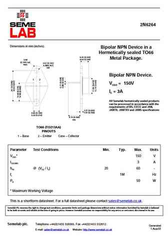
2N6264 Dimensions in mm (inches). Bipolar NPN Device in a Hermetically sealed TO66 6.35 (0.250) Metal Package. 8.64 (0.340) 3.68 (0.145) rad. 3.61 (0.142) max. 4.08(0.161) rad. Bipolar NPN Device. 1 2 VCEO = 150V IC = 3A All Semelab hermetically sealed products can be processed in accordance with the requirements of BS, CECC and JAN, JANTX, JANTXV and JANS speci
2n6271.pdf
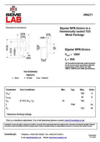
2N6271 Dimensions in mm (inches). Bipolar NPN Device in a Hermetically sealed TO3 25.15 (0.99) 6.35 (0.25) 26.67 (1.05) 9.15 (0.36) Metal Package. 10.67 (0.42) 11.18 (0.44) 1.52 (0.06) 3.43 (0.135) 1 2 Bipolar NPN Device. 3 VCEO = 100V (case) 3.84 (0.151) 4.09 (0.161) 7.92 (0.312) IC = 30A 12.70 (0.50) All Semelab hermetically sealed products can be processed in
2n6106 2n6107 2n6108 2n6109 2n6110 2n6111 2n6288 2n6289 2n6290 2n6291 2n6292 2n6293 2n6473 2n6474 2n6475 2n6476.pdf
Boca Semiconductor Corp. BSC http //www.bocasemi.com http //www.bocasemi.com
2n6107 2n6292.pdf
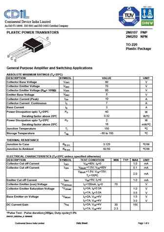
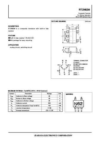
Continental Device India Limited An ISO/TS 16949, ISO 9001 and ISO 14001 Certified Company PLASTIC POWER TRANSISTORS 2N6107 PNP 2N6292 NPN TO-220 Plastic Package General Purpose Amplifier and Switching Applications ABSOLUTE MAXIMUM RATINGS (Ta=25 C) DESCRIPTION SYMBOL VALUE UNIT VCBO Collector Base Voltage 80 V Collector Emitter Voltage VCEO 70 V Collector Emitter Voltage (RBE= 100
2n6290.pdf
Continental Device India Limited An ISO/TS 16949, ISO 9001 and ISO 14001 Certified Company TO-220 Plastic Package 2N6290 2N6290 NPN PLASTIC POWER TRANSISTOR Complementary 2N6109 Medium Power Switching and Linear Applications PIN CONFIGURATION 4 1. BASE 2. COLLECTOR 3. EMITTER 4. COLLECTOR 1 2 3 C DIM MIN. MAX. B E F A 14.42 16.51 B 9.63 10.67 C 3.56 4.83 D0.90 E 1.15 1.40
2n6288.pdf
Continental Device India Limited An ISO/TS 16949, ISO 9001 and ISO 14001 Certified Company TO-220 Plastic Package 2N6288 2N6288 NPN PLASTIC POWER TRANSISTOR Complementary 2N6111 General Purpose Amplifier and Switching Applications PIN CONFIGURATION 4 1. BASE 2. COLLECTOR 3. EMITTER 4. COLLECTOR 1 2 3 C DIM MIN. MAX. B E F A 14.42 16.51 B 9.63 10.67 C 3.56 4.83 D0.90 E 1.1
2n6254.pdf
Product Specification www.jmnic.com Silicon NPN Power Transistors 2N6254 DESCRIPTION With TO-3 package Low saturation voltage Wide safe operating area High dissipation capability APPLICATIONS Series and shunt regulators High fidelity amplifiers Power switching circuits PINNING PIN DESCRIPTION 1 Base 2 Emitter 3 Collector Fig.1 simplified outline (TO-3)
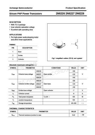
2n6226 2n6227 2n6228.pdf
Product Specification www.jmnic.com Silicon PNP Power Transistors 2N6226 2N6227 2N6228 DESCRIPTION With TO-3 package Low collector saturation voltage Excellent safe operating area APPLICATIONS For high power audio;stepping motor and other linear applications PINNING PIN DESCRIPTION 1 Base 2 Emitter 3 Collector Fig.1 simplified outline (TO-3) and symbol Absolut
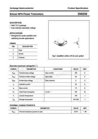
2n6258.pdf
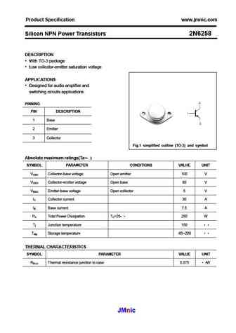
Product Specification www.jmnic.com Silicon NPN Power Transistors 2N6258 DESCRIPTION With TO-3 package Low collector-emitter saturation voltage APPLICATIONS Designed for audio amplifier and switching circuits applications PINNING PIN DESCRIPTION 1 Base 2 Emitter 3 Collector Fig.1 simplified outline (TO-3) and symbol Absolute maximum ratings(Ta= ) SYMBOL PARAME
2n6261.pdf
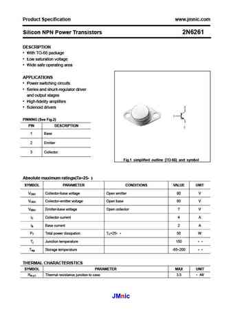
Product Specification www.jmnic.com Silicon NPN Power Transistors 2N6261 DESCRIPTION With TO-66 package Low saturation voltage Wide safe operating area APPLICATIONS Power switching circuits Series and shunt-regulator driver and output stages High-fidelity amplifers Solenoid drivers PINNING (See Fig.2) PIN DESCRIPTION 1 Base 2 Emitter 3 Collector Fig.
2n6249 2n6250 2n6251.pdf
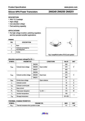
Product Specification www.jmnic.com Silicon NPN Power Transistors 2N6249 2N6250 2N6251 DESCRIPTION With TO-3 package High voltage Low saturation voltage Fast switching capability APPLICATIONS For high voltage inverters ,switching regulators and line operated amplifier applications PINNING PIN DESCRIPTION 1 Base Collector;connected to 2 mounting base 3 Em
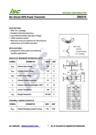
2n6216 2n6217.pdf
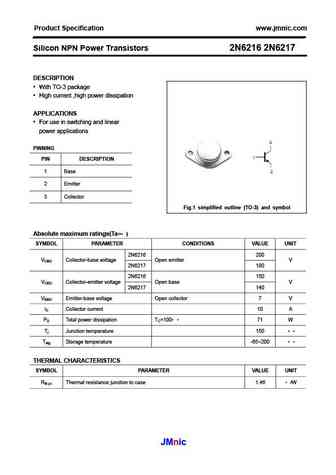
Product Specification www.jmnic.com Silicon NPN Power Transistors 2N6216 2N6217 DESCRIPTION With TO-3 package High current ,high power dissipation APPLICATIONS For use in switching and linear power applications PINNING PIN DESCRIPTION 1 Base 2 Emitter 3 Collector Fig.1 simplified outline (TO-3) and symbol Absolute maximum ratings(Ta= ) SYMBOL PARAMETER CONDITI
2n6294 2n6295.pdf
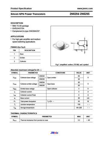
Product Specification www.jmnic.com Silicon NPN Power Transistors 2N6294 2N6295 DESCRIPTION With TO-66 package DARLINGTON Complement to type 2N6296/6297 APPLICATIONS For high gain amplifier and medium speed switching applications PINNING (See Fig.2) PIN DESCRIPTION 1 Base 2 Emitter 3 Collector Fig.1 simplified outline (TO-66) and symbol Absolute maximum rating
2n6257.pdf
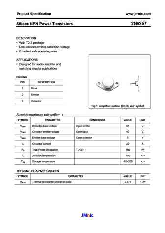
Product Specification www.jmnic.com Silicon NPN Power Transistors 2N6257 DESCRIPTION With TO-3 package Low collector-emitter saturation voltage Excellent safe operating area APPLICATIONS Designed for audio amplifier and switching circuits applications PINNING PIN DESCRIPTION 1 Base 2 Emitter 3 Collector Fig.1 simplified outline (TO-3) and symbol Absolute maxim
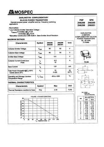
2n6298 2n6299.pdf
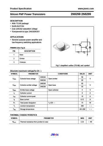
Product Specification www.jmnic.com Silicon PNP Power Transistors 2N6298 2N6299 DESCRIPTION With TO-66 package DARLINGTON Low collector saturation voltage Complement to type 2N6300/6301 APPLICATIONS General purpose power amplifier and low frequency switching applications PINNING (See Fig.2) PIN DESCRIPTION 1 Base 2 Emitter 3 Collector Fig.1 simplified outlin
2n6296 2n6297.pdf
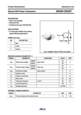
Product Specification www.jmnic.com Silicon PNP Power Transistors 2N6296 2N6297 DESCRIPTION With TO-66 package DARLINGTON Complement to type 2N6294/6295 APPLICATIONS For high gain amplifier and medium speed switching applications PINNING (See Fig.2) PIN DESCRIPTION 1 Base 2 Emitter 3 Collector Fig.1 simplified outline (TO-66) and symbol Absolute maximum ratings
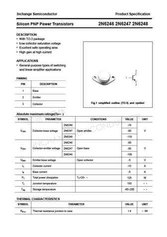
2n6246 2n6247 2n6248.pdf
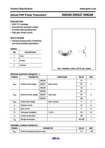
Product Specification www.jmnic.com Silicon PNP Power Transistors 2N6246 2N6247 2N6248 DESCRIPTION With TO-3 package Low collector saturation voltage Excellent safe operating area High gain at high current APPLICATIONS General-purpose types of switching and linear-amplifier applications PINNING PIN DESCRIPTION 1 Base 2 Emitter 3 Collector Fig.1 simplified ou
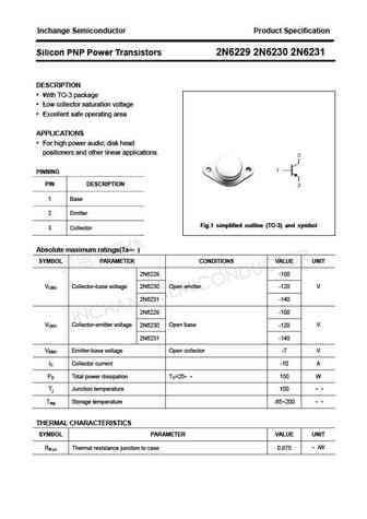
2n6229 2n6230 2n6231.pdf
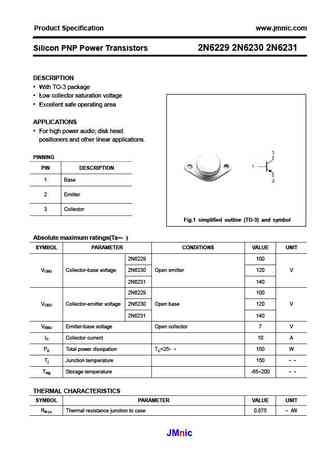
Product Specification www.jmnic.com Silicon PNP Power Transistors 2N6229 2N6230 2N6231 DESCRIPTION With TO-3 package Low collector saturation voltage Excellent safe operating area APPLICATIONS For high power audio; disk head positioners and other linear applications. PINNING PIN DESCRIPTION 1 Base 2 Emitter 3 Collector Fig.1 simplified outline (TO-3) and symbol
2n6253.pdf
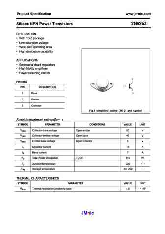
Product Specification www.jmnic.com Silicon NPN Power Transistors 2N6253 DESCRIPTION With TO-3 package Low saturation voltage Wide safe operating area High dissipation capability APPLICATIONS Series and shunt regulators High fidelity amplifiers Power switching circuits PINNING PIN DESCRIPTION 1 Base 2 Emitter 3 Collector Fig.1 simplified outline (TO-3)
2n6291 2n6293.pdf
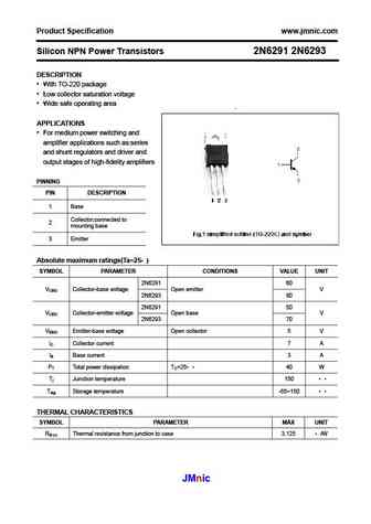
Product Specification www.jmnic.com Silicon NPN Power Transistors 2N6291 2N6293 DESCRIPTION With TO-220 package Low collector saturation voltage Wide safe operating area APPLICATIONS For medium power switching and amplifier applications such as series and shunt regulators and driver and output stages of high-fidelity amplifiers PINNING PIN DESCRIPTION 1 Base C
2n6260.pdf
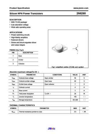
Product Specification www.jmnic.com Silicon NPN Power Transistors 2N6260 DESCRIPTION With TO-66 package Low saturation voltage Wide safe operating area APPLICATIONS Power switching circuits High-fidelity amplifers Solenoid drivers Series and shunt-regulator driver and output stages PINNING (See Fig.2) PIN DESCRIPTION 1 Base 2 Emitter 3 Collector Fig.
2n6259.pdf
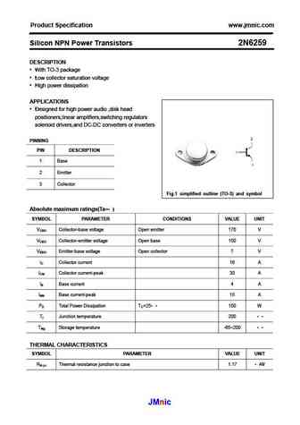
Product Specification www.jmnic.com Silicon NPN Power Transistors 2N6259 DESCRIPTION With TO-3 package Low collector saturation voltage High power dissipation APPLICATIONS Designed for high power audio ,disk head positioners,linear amplifiers,switching regulators solenoid drivers,and DC-DC converters or inverters PINNING PIN DESCRIPTION 1 Base 2 Emitter 3 Colle
2n6274 2n6277.pdf
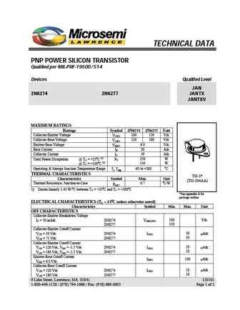
TECHNICAL DATA PNP POWER SILICON TRANSISTOR Qualified per MIL-PRF-19500/514 Devices Qualified Level JAN 2N6274 2N6277 JANTX JANTXV MAXIMUM RATINGS Ratings Symbol 2N6274 2N6277 Unit Collector-Emitter Voltage 100 150 Vdc VCEO Collector-Base Voltage 120 180 Vdc VCBO Emitter-Base Voltage 6.0 Vdc VEBO Base Current I 20 Adc B Collector Current 50 Adc IC 250 W T
2n6250t1.pdf

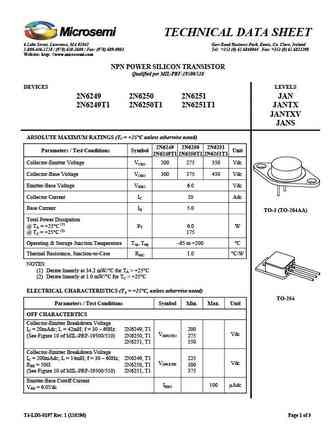
TECHNICAL DATA SHEET 6 Lake Street, Lawrence, MA 01841 Gort Road Business Park, Ennis, Co. Clare, Ireland 1-800-446-1158 / (978) 620-2600 / Fax (978) 689-0803 Tel +353 (0) 65 6840044 Fax +353 (0) 65 6822298 Website http //www.microsemi.com NPN POWER SILICON TRANSISTOR Qualified per MIL-PRF-19500/510 DEVICES LEVELS 2N6249 2N6250 2N6251 JAN 2N6249T1 2N6250T1 2N6251T1 JANTX JA
2n6232.pdf
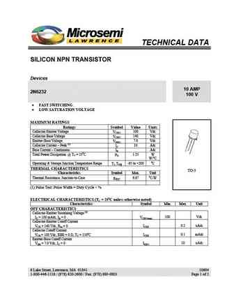
TECHNICAL DATA SILICON NPN TRANSISTOR Devices 10 AMP 2N6232 100 V FAST SWITCHING LOW SATURATION VOLTAGE MAXIMUM RATINGS Ratings Symbol Value Units Collector-Emitter Voltage 100 Vdc VCEO Collector-Base Voltage 140 Vdc VCBO Emitter-Base Voltage 7.0 Vdc VEBO Collector Current Peak (1) 10 Adc IC Base Current Continuous IB Adc Total Power Dissipation @
2n6251t1.pdf
TECHNICAL DATA SHEET 6 Lake Street, Lawrence, MA 01841 Gort Road Business Park, Ennis, Co. Clare, Ireland 1-800-446-1158 / (978) 620-2600 / Fax (978) 689-0803 Tel +353 (0) 65 6840044 Fax +353 (0) 65 6822298 Website http //www.microsemi.com NPN POWER SILICON TRANSISTOR Qualified per MIL-PRF-19500/510 DEVICES LEVELS 2N6249 2N6250 2N6251 JAN 2N6249T1 2N6250T1 2N6251T1 JANTX JA
2n6255.pdf
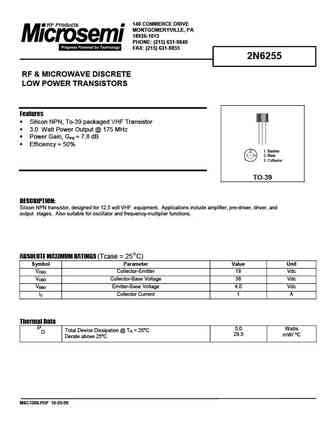
140 COMMERCE DRIVE MONTGOMERYVILLE, PA 18936-1013 PHONE (215) 631-9840 FAX (215) 631-9855 2N6255 RF & MICROWAVE DISCRETE LOW POWER TRANSISTORS Features Silicon NPN, To-39 packaged VHF Transistor 3.0 Watt Power Output @ 175 MHz Power Gain, GPE = 7.8 dB Efficiency = 50% 1. Emitter 2. Base 3. Collector TO-39 DESCRIPTION Silicon NPN transistor, designed for 12.5
2n6249t1 2n6249t1 2n6250t1.pdf

TECHNICAL DATA SHEET 6 Lake Street, Lawrence, MA 01841 Gort Road Business Park, Ennis, Co. Clare, Ireland 1-800-446-1158 / (978) 620-2600 / Fax (978) 689-0803 Tel +353 (0) 65 6840044 Fax +353 (0) 65 6822298 Website http //www.microsemi.com NPN POWER SILICON TRANSISTOR Qualified per MIL-PRF-19500/510 DEVICES LEVELS 2N6249 2N6250 2N6251 JAN 2N6249T1 2N6250T1 2N6251T1 JANTX JA
2n6249 2n6250 2n6251.pdf
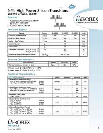
NPN High Power Silicon Transistors 2N6249, 2N6250, 2N6251 Features Available in JAN, JANTX, and JANTXV per MIL-PRF-19500/371 TO-3 (TO-204AA) Package Maximum Ratings Ratings Symbol 2N6249 2N6250 2N6251 Units Collector - Emitter Voltage VCEO 200 275 350 Vdc Collector - Base Voltage VCBO 300 375 450 Vdc Emitter - Base Voltage VEBO 6.0 Vdc Collector Current IC 10 Adc Base Curr
2n6298 2n6299.pdf
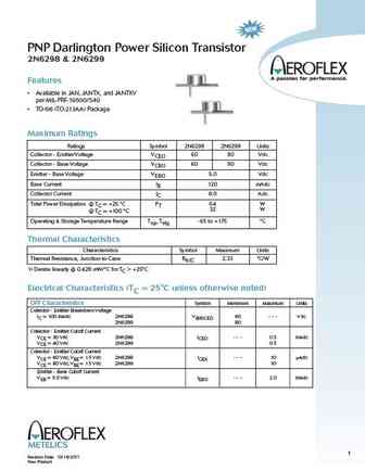
PNP Darlington Power Silicon Transistor 2N6298 & 2N6299 Features Available in JAN, JANTX, and JANTXV per MIL-PRF-19500/540 TO-66 (TO-213AA) Package Maximum Ratings Ratings Symbol 2N6298 2N6299 Units Collector - Emitter Voltage VCEO 60 80 Vdc Collector - Base Voltage VCBO 60 80 Vdc Emitter - Base Voltage VEBO 5.0 Vdc Base Current IB 120 mAdc Collector Current IC 8.0 Adc Tot
2n6286 2n6287.pdf
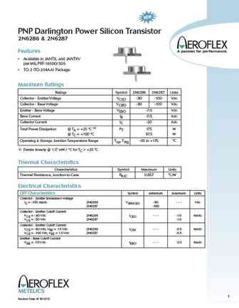
PNP Darlington Power Silicon Transistor 2N6286 & 2N6287 Features Available in JANTX, and JANTXV per MIL-PRF-19500/505 TO-3 (TO-204AA) Package Maximum Ratings Ratings Symbol 2N6286 2N6287 Units Collector - Emitter Voltage VCEO -80 -100 Vdc Collector - Base Voltage VCBO -80 -100 Vdc Emitter - Base Voltage VEBO -7.0 Vdc Base Current IB -0.5 Adc Collector Current IC -20 Adc (1
2n6254.pdf
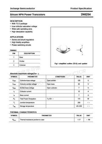
Inchange Semiconductor Product Specification Silicon NPN Power Transistors 2N6254 DESCRIPTION With TO-3 package Low collector saturation voltage Wide safe operating area High dissipation capability APPLICATIONS Series and shunt regulators High fidelity amplifiers Power switching circuits PINNING PIN DESCRIPTION 1 Base 2 Emitter Fig.1 simplified outline
2n6290.pdf
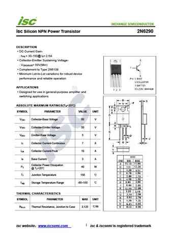
isc Silicon NPN Power Transistor 2N6290 DESCRIPTION DC Current Gain- h = 30-150@ I = 2.5A FE C Collector-Emitter Sustaining Voltage- V = 50V(Min) CEO(SUS) Complement to Type 2N6109 Minimum Lot-to-Lot variations for robust device performance and reliable operation APPLICATIONS Designed for use in general-purpose amplifier and switching applications ABSOLUTE MAXIMUM RA
2n6262.pdf
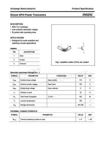
Inchange Semiconductor Product Specification Silicon NPN Power Transistors 2N6262 DESCRIPTION With TO-3 package Low collector saturation voltage Excellent safe operating area APPLICATIONS Designed for audio amplifier and switching circuits applications PINNING PIN DESCRIPTION 1 Base 2 Emitter Fig.1 simplified outline (TO-3) and symbol 3 Collector Absolute maxi
2n6287.pdf
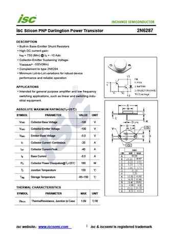
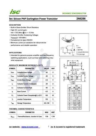
INCHANGE Semiconductor isc Silicon PNP Darlingtion Power Transistor 2N6287 DESCRIPTION Built-in Base-Emitter Shunt Resistors High DC current gain- h = 750 (Min) @ I = -10 Adc FE C Collector-Emitter Sustaining Voltage- V = -100V(Min) CEO(SUS) Complement to type 2N6284 Minimum Lot-to-Lot variations for robust device performance and reliable operation APPLICATIONS Intende
2n6226 2n6227 2n6228.pdf
Inchange Semiconductor Product Specification Silicon PNP Power Transistors 2N6226 2N6227 2N6228 DESCRIPTION With TO-3 package Low collector saturation voltage Excellent safe operating area APPLICATIONS For high power audio;stepping motor and other linear applications PINNING PIN DESCRIPTION 1 Base 2 Emitter Fig.1 simplified outline (TO-3) and symbol 3 Collector
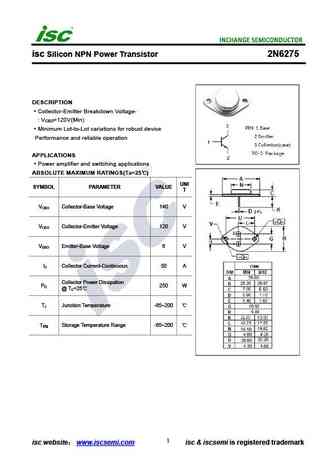
2n6276.pdf

isc Silicon NPN Power Transistor 2N6276 DESCRIPTION Collector-Emitter Breakdown Voltage- V =140V(Min) CEO Minimum Lot-to-Lot variations for robust device Performance and reliable operation APPLICATIONS Power amplifier and switching applications ABSOLUTE MAXIMUM RATINGS(Ta=25 ) UNI SYMBOL PARAMETER VALUE T V Collector-Base Voltage 160 V CBO V Collector-Emitter Voltage 14
2n6258.pdf
Inchange Semiconductor Product Specification Silicon NPN Power Transistors 2N6258 DESCRIPTION With TO-3 package Low collector saturation voltage APPLICATIONS Designed for audio amplifier and switching circuits applications PINNING PIN DESCRIPTION 1 Base 2 Emitter Fig.1 simplified outline (TO-3) and symbol 3 Collector Absolute maximum ratings(Ta= ) SYMBOL PARAM
2n6292.pdf
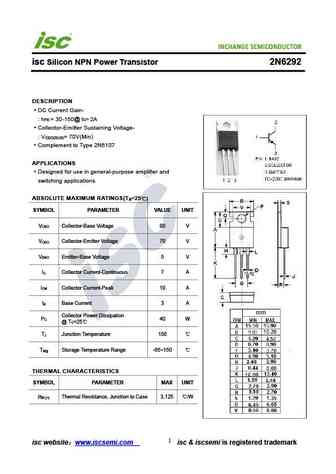
isc Product Specification isc Silicon NPN Power Transistor 2N6292 DESCRIPTION DC Current Gain- h = 30-150@ I = 2A FE C Collector-Emitter Sustaining Voltage- V = 70V(Min) CEO(SUS) Complement to Type 2N6107 APPLICATIONS Designed for use in general-purpose amplifier and switching applications ABSOLUTE MAXIMUM RATINGS(T =25 ) a SYMBOL PARAMETER VALUE UNIT V Collector-B
2n6285 2n6286 2n6287.pdf
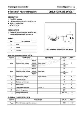
Inchange Semiconductor Product Specification Silicon PNP Power Transistors 2N6285 2N6286 2N6287 DESCRIPTION With TO-3 package Complement to type 2N6282/6283/6284 High DC current gain DARLINGTON APPLICATIONS For use in general-purpose amplifier and low-frequency switching applications PINNING PIN DESCRIPTION 1 Base 2 Emitter Fig.1 simplified outline (TO-3) and
2n6261.pdf
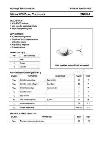
Inchange Semiconductor Product Specification Silicon NPN Power Transistors 2N6261 DESCRIPTION With TO-66 package Low collector saturation voltage Wide safe operating area APPLICATIONS Power switching circuits Series and shunt-regulator driver and output stages High-fidelity amplifers Solenoid drivers PINNING (See Fig.2) PIN DESCRIPTION 1 Base 2 Emitter
2n6289.pdf

isc Silicon NPN Power Transistor 2N6289 DESCRIPTION DC Current Gain- h = 30-150@ I = 3A FE C Collector-Emitter Sustaining Voltage- V = 30V(Min) CEO(SUS) Minimum Lot-to-Lot variations for robust device performance and reliable operation APPLICATIONS Designed for use in general-purpose amplifier and switching applications ABSOLUTE MAXIMUM RATINGS(T =25 ) a SYMBOL PARA
2n6211.pdf
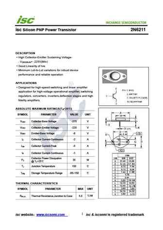
INCHANGE Semiconductor isc Silicon PNP Power Transistor 2N6211 DESCRIPTION High Collector-Emitter Sustaining Voltage- V = -225V(Min) CEO(SUS) Good Linearity of h FE Minimum Lot-to-Lot variations for robust device performance and reliable operation APPLICATIONS Designed for high-speed switching and linear amplifier application for high-voltage operational amplifier, switchi
2n6274.pdf

isc Silicon NPN Power Transistor 2N6274 DESCRIPTION Collector-Emitter Breakdown Voltage- V =100V(Min) CEO Minimum Lot-to-Lot variations for robust device Performance and reliable operation APPLICATIONS Power amplifier and switching applications ABSOLUTE MAXIMUM RATINGS(Ta=25 ) UNI SYMBOL PARAMETER VALUE T V Collector-Base Voltage 120 V CBO V Collector-Emitter Voltage 10
2n6249 2n6250 2n6251.pdf
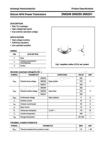
Inchange Semiconductor Product Specification Silicon NPN Power Transistors 2N6249 2N6250 2N6251 DESCRIPTION With TO-3 package High voltage,high speed Low collector saturation voltage APPLICATIONS High voltage inverters Switching regulators Line operated amplifier PINNING PIN DESCRIPTION 1 Base Collector;connected to 2 mounting base Fig.1 simplified out
2n6293.pdf
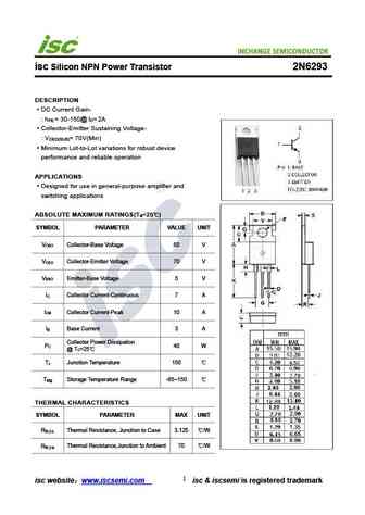
isc Silicon NPN Power Transistor 2N6293 DESCRIPTION DC Current Gain- h = 30-150@ I = 2A FE C Collector-Emitter Sustaining Voltage- V = 70V(Min) CEO(SUS) Minimum Lot-to-Lot variations for robust device performance and reliable operation APPLICATIONS Designed for use in general-purpose amplifier and switching applications ABSOLUTE MAXIMUM RATINGS(T =25 ) a SYMBOL PARA
2n6288 2n6290 2n6292.pdf
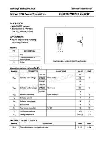
Inchange Semiconductor Product Specification Silicon NPN Power Transistors 2N6288 2N6290 2N6292 DESCRIPTION With TO-220 package Complement to PNP type 2N6107; 2N6109 ;2N6111 APPLICATIONS Power amplifier and switching circuits applications PINNING PIN DESCRIPTION 1 Base Collector;connected to 2 mounting base 3 Emitter Absolute maximum ratings(Ta=25 ) SYM
2n6216 2n6217.pdf
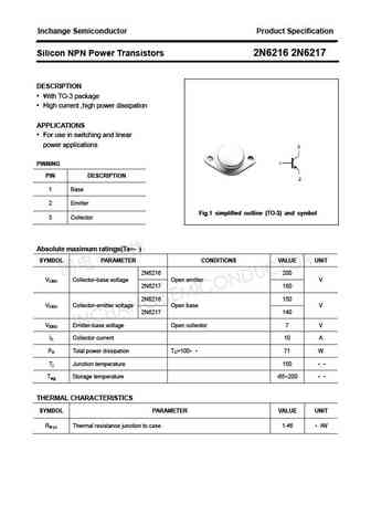
Inchange Semiconductor Product Specification Silicon NPN Power Transistors 2N6216 2N6217 DESCRIPTION With TO-3 package High current ,high power dissipation APPLICATIONS For use in switching and linear power applications PINNING PIN DESCRIPTION 1 Base 2 Emitter Fig.1 simplified outline (TO-3) and symbol 3 Collector Absolute maximum ratings(Ta= ) SYMBOL PARAMETE
2n6278.pdf
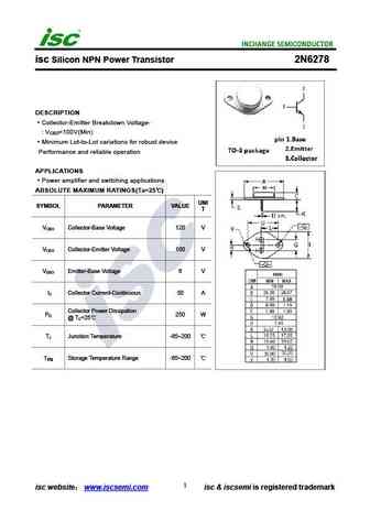
isc Silicon NPN Power Transistor 2N6278 DESCRIPTION Collector-Emitter Breakdown Voltage- V =100V(Min) CEO Minimum Lot-to-Lot variations for robust device Performance and reliable operation APPLICATIONS Power amplifier and switching applications ABSOLUTE MAXIMUM RATINGS(Ta=25 ) UNI SYMBOL PARAMETER VALUE T V Collector-Base Voltage 120 V CBO V Collector-Emitter Voltage 10
2n6282 2n6283 2n6284.pdf
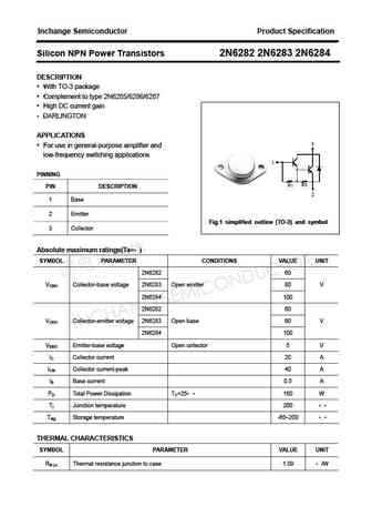
Inchange Semiconductor Product Specification Silicon NPN Power Transistors 2N6282 2N6283 2N6284 DESCRIPTION With TO-3 package Complement to type 2N6285/6286/6287 High DC current gain DARLINGTON APPLICATIONS For use in general-purpose amplifier and low-frequency switching applications PINNING PIN DESCRIPTION 1 Base 2 Emitter Fig.1 simplified outline (TO-3) and
2n6294 2n6295.pdf
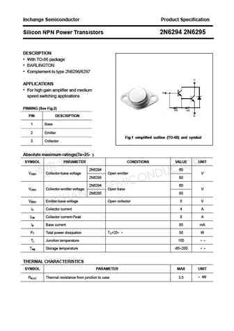
Inchange Semiconductor Product Specification Silicon NPN Power Transistors 2N6294 2N6295 DESCRIPTION With TO-66 package DARLINGTON Complement to type 2N6296/6297 APPLICATIONS For high gain amplifier and medium speed switching applications PINNING (See Fig.2) PIN DESCRIPTION 1 Base 2 Emitter Fig.1 simplified outline (TO-66) and symbol 3 Collector Absolute maximu
2n6217.pdf
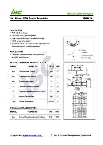
isc Silicon NPN Power Transistor 2N6217 DESCRIPTION With TO-3 package Excellent Safe Operating Area Low Collector-Emitter Saturation Voltage 100% avalanche tested Minimum Lot-to-Lot variations for robust device performance and reliable operation. APPLICATIONS Designed for linear power and switching amplifier applications. ABSOLUTE MAXIMUM RATINGS(T =25 ) a SYMBOL PARA
2n6257.pdf
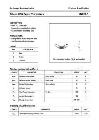
Inchange Semiconductor Product Specification Silicon NPN Power Transistors 2N6257 DESCRIPTION With TO-3 package Low collector saturation voltage Excellent safe operating area APPLICATIONS Designed for audio amplifier and switching circuits applications PINNING PIN DESCRIPTION 1 Base 2 Emitter Fig.1 simplified outline (TO-3) and symbol 3 Collector Absolute maxi
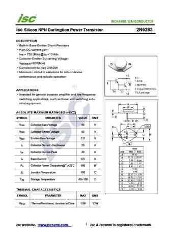
2n6284.pdf
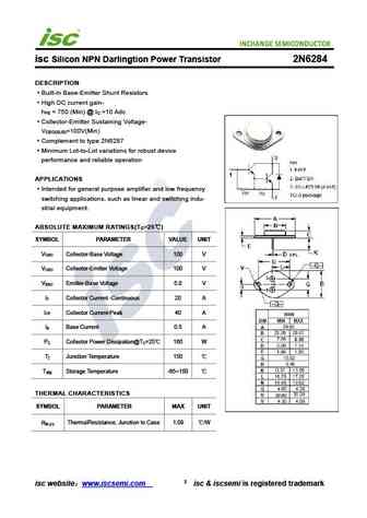
isc Silicon NPN Darlingtion Power Transistor 2N6284 DESCRIPTION Built-in Base-Emitter Shunt Resistors High DC current gain- h = 750 (Min) @ I =10 Adc FE C Collector-Emitter Sustaining Voltage- V =100V(Min) CEO(SUS) Complement to type 2N6287 Minimum Lot-to-Lot variations for robust device performance and reliable operation APPLICATIONS Intended for general purpose amplif
2n6280.pdf

isc Silicon NPN Power Transistor 2N6280 DESCRIPTION Collector-Emitter Breakdown Voltage- V =140V(Min) CEO Minimum Lot-to-Lot variations for robust device Performance and reliable operation APPLICATIONS Power amplifier and switching applications ABSOLUTE MAXIMUM RATINGS(Ta=25 ) UNI SYMBOL PARAMETER VALUE T V Collector-Base Voltage 160 V CBO V Collector-Emitter Voltage 14
2n6235.pdf
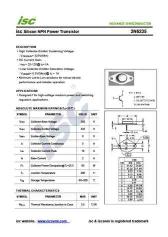
isc Silicon NPN Power Transistor 2N6235 DESCRIPTION High Collector-Emitter Sustaining Voltage- V = 325V(Min) CEO(SUS) DC Current Gain- h = 25-125@ I = 1A FE C Low Collector-Emitter Saturation Voltage- V )= 0.5V(Max)@ I = 1A CE(sat C Minimum Lot-to-Lot variations for robust device performance and reliable operation APPLICATIONS Designed f for high-voltage medium pow
2n6263 2n6264.pdf
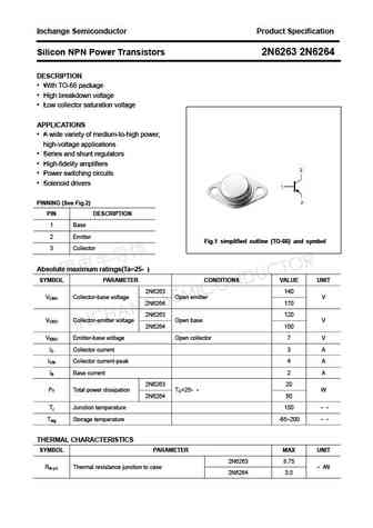
Inchange Semiconductor Product Specification Silicon NPN Power Transistors 2N6263 2N6264 DESCRIPTION With TO-66 package High breakdown voltage Low collector saturation voltage APPLICATIONS A wide variety of medium-to-high power, high-voltage applications Series and shunt regulators High-fidelity amplifiers Power switching circuits Solenoid drivers PINNI
2n6298 2n6299.pdf
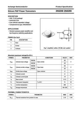
Inchange Semiconductor Product Specification Silicon PNP Power Transistors 2N6298 2N6299 DESCRIPTION With TO-66 package DARLINGTON Low collector saturation voltage Complement to type 2N6300/6301 APPLICATIONS General purpose power amplifier and low frequency switching applications PINNING (See Fig.2) PIN DESCRIPTION 1 Base 2 Emitter Fig.1 simplified outline (T
2n6277.pdf
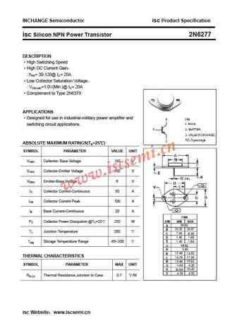
INCHANGE Semiconductor isc Product Specification isc Silicon NPN Power Transistor 2N6277 DESCRIPTION High Switching Speed High DC Current Gain- hFE= 30-120@ IC= 20A Low Collector Saturation Voltage- VCE(sat)=1.0V(Min.)@ IC= 20A Complement to Type 2N6379 APPLICATIONS Designed for use in industrial-military power amplifier and switching circuit applications.
2n6216.pdf
isc Silicon NPN Power Transistor 2N6216 DESCRIPTION With TO-3 package Excellent Safe Operating Area Low Collector-Emitter Saturation Voltage 100% avalanche tested Minimum Lot-to-Lot variations for robust device performance and reliable operation. APPLICATIONS Designed for linear power and switching amplifier applications. ABSOLUTE MAXIMUM RATINGS(T =25 ) a SYMBOL PARA
2n6296 2n6297.pdf
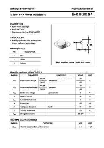
Inchange Semiconductor Product Specification Silicon PNP Power Transistors 2N6296 2N6297 DESCRIPTION With TO-66 package DARLINGTON Complement to type 2N6294/6295 APPLICATIONS For high gain amplifier and medium speed switching applications PINNING (See Fig.2) PIN DESCRIPTION 1 Base 2 Emitter Fig.1 simplified outline (TO-66) and symbol 3 Collector Absolute maximu
2n6282.pdf
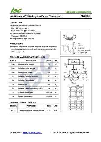
isc Silicon NPN Darlingtion Power Transistor 2N6282 DESCRIPTION Built-in Base-Emitter Shunt Resistors High DC current gain- h = 750 (Min) @ I = 10 Adc FE C Collector-Emitter Sustaining Voltage- V = 60V(Min) CEO(SUS) Complement to type 2N6285 APPLICATIONS Intended for general purpose amplifier and low frequency switching applications, such as linear and switching indu- str
2n6286.pdf
isc Silicon PNP Darlingtion Power Transistor 2N6286 DESCRIPTION Built-in Base-Emitter Shunt Resistors High DC current gain- h = 750 (Min) @ I = -10 Adc FE C Collector-Emitter Sustaining Voltage- V = -80V(Min) CEO(SUS) Complement to type 2N6283 Minimum Lot-to-Lot variations for robust device performance and reliable operation APPLICATIONS Intended for general purpose amp
2n6246 2n6247 2n6248.pdf
Inchange Semiconductor Product Specification Silicon PNP Power Transistors 2N6246 2N6247 2N6248 DESCRIPTION With TO-3 package Low collector saturation voltage Excellent safe operating area High gain at high current APPLICATIONS General-purpose types of switching and linear-amplifier applications PINNING PIN DESCRIPTION 1 Base 2 Emitter Fig.1 simplified outlin
2n6275.pdf
isc Silicon NPN Power Transistor 2N6275 DESCRIPTION Collector-Emitter Breakdown Voltage- V =120V(Min) CEO Minimum Lot-to-Lot variations for robust device Performance and reliable operation APPLICATIONS Power amplifier and switching applications ABSOLUTE MAXIMUM RATINGS(Ta=25 ) UNI SYMBOL PARAMETER VALUE T V Collector-Base Voltage 140 V CBO V Collector-Emitter Voltage 12
2n6229 2n6230 2n6231.pdf
Inchange Semiconductor Product Specification Silicon PNP Power Transistors 2N6229 2N6230 2N6231 DESCRIPTION With TO-3 package Low collector saturation voltage Excellent safe operating area APPLICATIONS For high power audio; disk head positioners and other linear applications. PINNING PIN DESCRIPTION 1 Base 2 Emitter Fig.1 simplified outline (TO-3) and symbol 3
2n6283.pdf
isc Silicon NPN Darlingtion Power Transistor 2N6283 DESCRIPTION Built-in Base-Emitter Shunt Resistors High DC current gain- h = 750 (Min) @ I =10 Adc FE C Collector-Emitter Sustaining Voltage- V =80V(Min) CEO(SUS) Complement to type 2N6286 Minimum Lot-to-Lot variations for robust device performance and reliable operation APPLICATIONS Intended for general purpose amplifi
2n6253.pdf
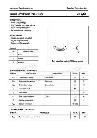
Inchange Semiconductor Product Specification Silicon NPN Power Transistors 2N6253 DESCRIPTION With TO-3 package Low collector saturation voltage Wide safe operating area High dissipation capability APPLICATIONS Series and shunt regulators High fidelity amplifiers Power switching circuits PINNING PIN DESCRIPTION 1 Base 2 Emitter Fig.1 simplified outline
2n6291 2n6293.pdf
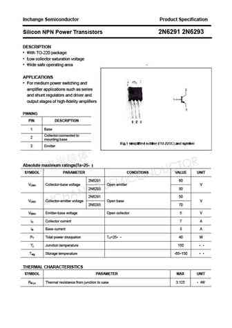
Inchange Semiconductor Product Specification Silicon NPN Power Transistors 2N6291 2N6293 DESCRIPTION With TO-220 package Low collector saturation voltage Wide safe operating area APPLICATIONS For medium power switching and amplifier applications such as series and shunt regulators and driver and output stages of high-fidelity amplifiers PINNING PIN DESCRIPTION 1
2n6212.pdf
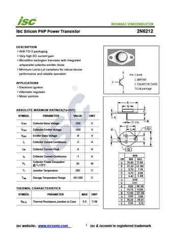
INCHANGE Semiconductor isc Silicon PNP Power Transistor 2N6212 DESCRIPTION With TO-3 packaging Very high DC current gain Monolithic darlington transistor with integrated antiparallel collector-emitter diode Minimum Lot-to-Lot variations for robust device performance and reliable operation APPLICATIONS Electronic ignition Alternator regulator Motor controls ABSOLUTE MA
2n6291.pdf

isc Silicon NPN Power Transistor 2N6291 DESCRIPTION DC Current Gain- h = 30-150@ I = 2.5A FE C Collector-Emitter Sustaining Voltage- V = 50V(Min) CEO(SUS) Minimum Lot-to-Lot variations for robust device performance and reliable operation APPLICATIONS Designed for use in general-purpose amplifier and switching applications ABSOLUTE MAXIMUM RATINGS(T =25 ) a SYMBOL PA
2n6260.pdf
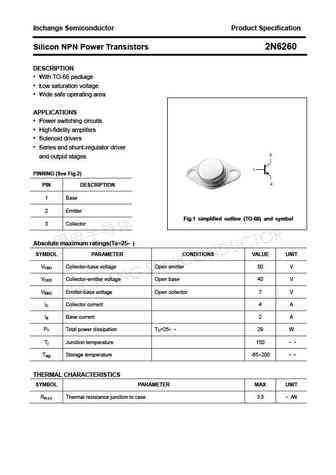
Inchange Semiconductor Product Specification Silicon NPN Power Transistors 2N6260 DESCRIPTION With TO-66 package Low saturation voltage Wide safe operating area APPLICATIONS Power switching circuits High-fidelity amplifers Solenoid drivers Series and shunt-regulator driver and output stages PINNING (See Fig.2) PIN DESCRIPTION 1 Base 2 Emitter Fig.1 si
2n6270 2n6271.pdf
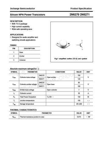
Inchange Semiconductor Product Specification Silicon NPN Power Transistors 2N6270 2N6271 DESCRIPTION With TO-3 package High current capability Wide safe operating area APPLICATIONS Designed for audio amplifier and switching circuits applications PINNING PIN DESCRIPTION 1 Base 2 Emitter Fig.1 simplified outline (TO-3) and symbol 3 Collector Absolute maximum rat
2n6259.pdf
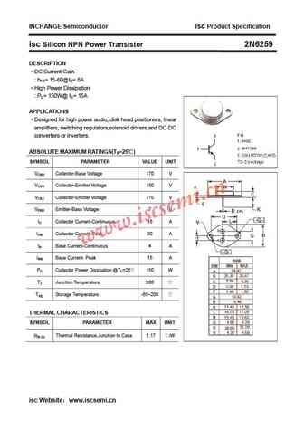
INCHANGE Semiconductor isc Product Specification isc Silicon NPN Power Transistor 2N6259 DESCRIPTION DC Current Gain- hFE= 15-60@IC= 8A High Power Dissipation PD= 150W@ IC= 15A APPLICATIONS Designed for high power audio, disk head positioners, linear amplifiers, switching regulators,solenoid drivers,and DC-DC converters or inverters. ABSOLUTE MAXIMUM RATINGS(T
2n6251.pdf
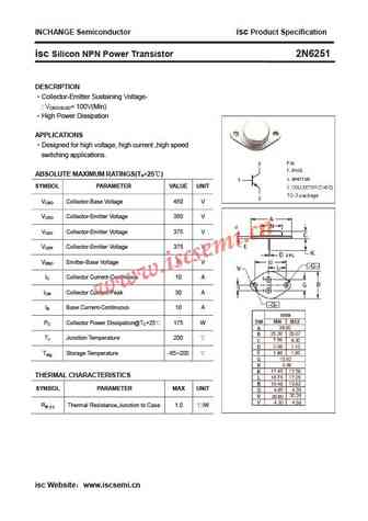
INCHANGE Semiconductor isc Product Specification isc Silicon NPN Power Transistor 2N6251 DESCRIPTION Collector-Emitter Sustaining Voltage- VCEO(SUS)= 100V(Min) High Power Dissipation APPLICATIONS Designed for high voltage, high current ,high speed switching applications. ABSOLUTE MAXIMUM RATINGS(Ta=25 ) SYMBOL PARAMETER VALUE UNIT V Collector-Base Voltage 450 V
2n6213.pdf
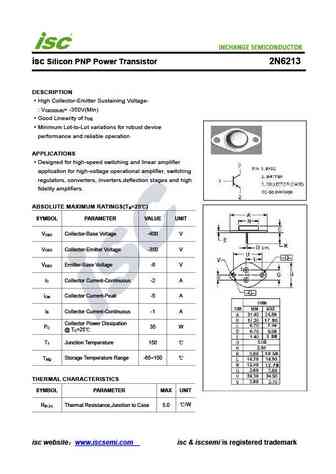
isc Silicon PNP Power Transistor 2N6213 DESCRIPTION High Collector-Emitter Sustaining Voltage- V = -350V(Min) CEO(SUS) Good Linearity of h FE Minimum Lot-to-Lot variations for robust device performance and reliable operation APPLICATIONS Designed for high-speed switching and linear amplifier application for high-voltage operational amplifier, switching regulators, converte
2n6281.pdf
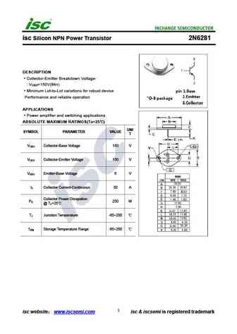
isc Silicon NPN Power Transistor 2N6281 DESCRIPTION Collector-Emitter Breakdown Voltage- V =150V(Min) CEO Minimum Lot-to-Lot variations for robust device Performance and reliable operation APPLICATIONS Power amplifier and switching applications ABSOLUTE MAXIMUM RATINGS(Ta=25 ) UNI SYMBOL PARAMETER VALUE T V Collector-Base Voltage 180 V CBO V Collector-Emitter Voltage 15
Otros transistores... 2N6195 , 2N6196 , 2N6197 , 2N6198 , 2N6199 , 2N61A , 2N61B , 2N61C , 2222A , 2N620 , 2N6200 , 2N6201 , 2N6202 , 2N6203 , 2N6204 , 2N6205 , 2N6206 .
History: 2N61A | 2N4125
🌐 : EN ES РУ

Liste
Recientemente añadidas las descripciónes de los transistores:
BJT: GA1A4M | SBT42 | 2SA200-Y | 2SA200-O | 2SD882-Q | 2SD882-P | 2SD882-E | 2SC945-L | 2SC945-H | 2SC4226-R23 | 2SC3357-F | 2SC3357-E | 2SC3356-R26 | 2SC3356-R24 | 2SC3356-R23 | 2SB772-Q | 2SB772-P | 2SB772-E | 2SA1015-L | 2SA1015-H | HSS8550
Popular searches
mosfet k8a50d | sl100 transistor | d2499 datasheet | 6r190p6 datasheet | 2n270 | 2n2924 | mpsa65 | 2sa794