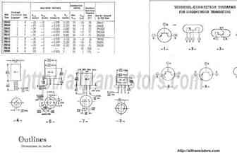
2N64 Equivalente. Reemplazo. Hoja de especificaciones. Principales características
Número de Parte: 2N64
Material: Ge
Polaridad de transistor: PNP
ESPECIFICACIONES MÁXIMAS
Disipación total del dispositivo (Pc): 0.12 W
Tensión colector-base (Vcb): 25 V
Tensión colector-emisor (Vce): 22 V
Tensión emisor-base (Veb): 12 V
Corriente del colector DC máxima (Ic): 0.01 A
Temperatura operativa máxima (Tj): 85 °C
CARACTERÍSTICAS ELÉCTRICAS
Transición de frecuencia (fT): 0.15 MHz
Ganancia de corriente contínua (hFE): 50
Encapsulados: TO22
Búsqueda de reemplazo de 2N64
- Selecciónⓘ de transistores por parámetros
2N64 datasheet
2n6439re.pdf
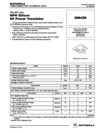
MOTOROLA Order this document SEMICONDUCTOR TECHNICAL DATA by 2N6439/D The RF Line NPN Silicon 2N6439 RF Power Transistor . . . designed primarily for wideband large signal output amplifier stages in the 225 to 400 MHz frequency range. Guaranteed Performance in 225 to 400 MHz Broadband Amplifier @ 28 Vdc Output Power = 60 Watts over 225 to 400 MHz Band 60 W, 225 to 400 MHz Min
2n6487 2n6488 2n6490 2n6491.pdf
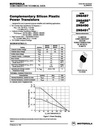
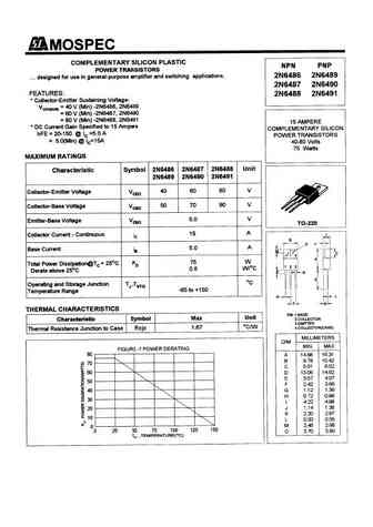
Order this document MOTOROLA by 2N6487/D SEMICONDUCTOR TECHNICAL DATA NPN 2N6487 Complementary Silicon Plastic Power Transistors * 2N6488 PNP . . . designed for use in general purpose amplifier and switching applications. DC Current Gain Specified to 15 Amperes 2N6490 hFE = 20 150 @ IC = 5.0 Adc hFE = 5.0 (Min) @ IC = 15 Adc 2N6491* Collector Emitter Sustaining
2n6426 2n6427.pdf
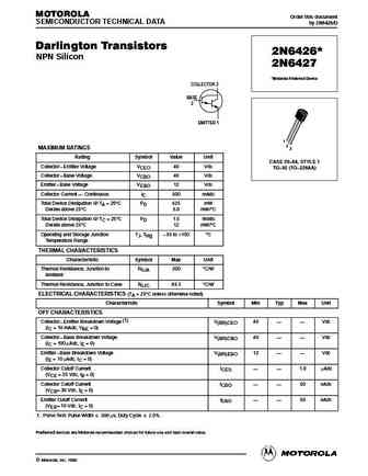
MOTOROLA Order this document SEMICONDUCTOR TECHNICAL DATA by 2N6426/D Darlington Transistors 2N6426* NPN Silicon 2N6427 *Motorola Preferred Device COLLECTOR 3 BASE 2 EMITTER 1 1 2 MAXIMUM RATINGS 3 Rating Symbol Value Unit CASE 29 04, STYLE 1 Collector Emitter Voltage VCEO 40 Vdc TO 92 (TO 226AA) Collector Base Voltage VCBO 40 Vdc Emitter Base Voltage VEBO 12 Vd
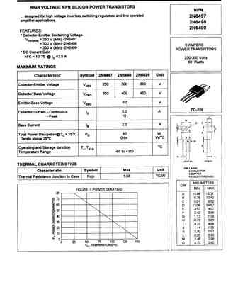
2n6497 2n6498.pdf
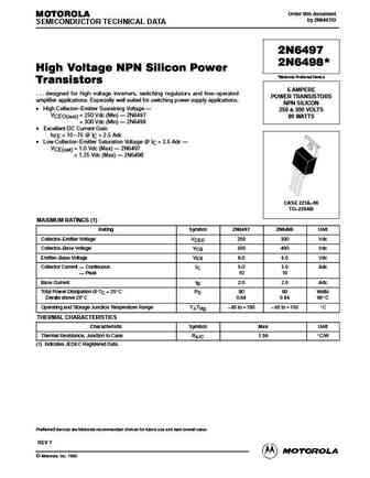
Order this document MOTOROLA by 2N6497/D SEMICONDUCTOR TECHNICAL DATA 2N6497 2N6498* High Voltage NPN Silicon Power *Motorola Preferred Device Transistors 5 AMPERE . . . designed for high voltage inverters, switching regulators and line operated POWER TRANSISTORS amplifier applications. Especially well suited for switching power supply applications. NPN SILICON High Collecto
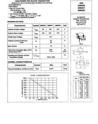
2n6436 2n6437 2n6438.pdf
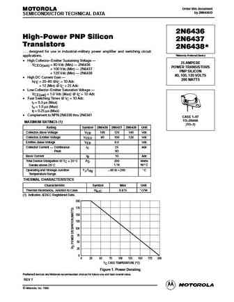
Order this document MOTOROLA by 2N6436/D SEMICONDUCTOR TECHNICAL DATA 2N6436 High-Power PNP Silicon 2N6437 Transistors 2N6438 * . . . designed for use in industrial military power amplifier and switching circuit *Motorola Preferred Device applications. High Collector Emitter Sustaining Voltage 25 AMPERE VCEO(sus) = 80 Vdc (Min) 2N6436 POWER TRANSISTORS VCEO(sus)
2n6427 1.pdf
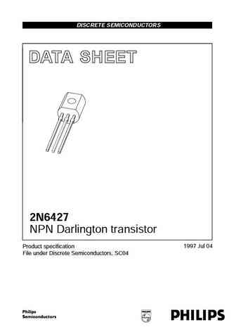
DISCRETE SEMICONDUCTORS DATA SHEET book, halfpage M3D186 2N6427 NPN Darlington transistor 1997 Jul 04 Product specification File under Discrete Semiconductors, SC04 Philips Semiconductors Product specification NPN Darlington transistor 2N6427 FEATURES PINNING High current (max. 500 mA) PIN DESCRIPTION Low voltage (max. 30 V) 1 collector High DC current gain (min. 10
2n6487 2n6488 2n6490.pdf
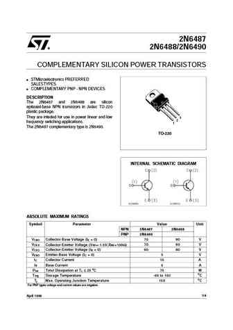
2N6487 2N6488/2N6490 COMPLEMENTARY SILICON POWER TRANSISTORS STMicroelectronics PREFERRED SALESTYPES COMPLEMENTARY PNP - NPN DEVICES DESCRIPTION The 2N6487 and 2N6488 are silicon epitaxial-base NPN transistors in Jedec TO-220 plastic package. They are inteded for use in power linear and low 3 2 frequency switching applications. 1 The 2N6487 complementary type is 2N6490.
2n6426.pdf
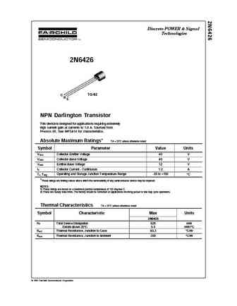
Discrete POWER & Signal Technologies 2N6426 C TO-92 B E NPN Darlington Transistor This device is designed for applications requiring extremely high current gain at currents to 1.0 A. Sourced from Process 05. See MPSA14 for characteristics. Absolute Maximum Ratings* TA = 25 C unless otherwise noted Symbol Parameter Value Units VCEO Collector-Emitter Voltage 40 V V Collector-Base Vo
2n6427 mmbt6427.pdf
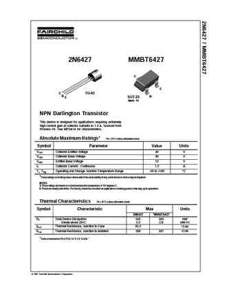
2N6427 MMBT6427 C E C TO-92 B B SOT-23 E Mark 1V NPN Darlington Transistor This device is designed for applications requiring extremely high current gain at collector currents to 1.0 A. Sourced from Process 05. See MPSA14 for characteristics. Absolute Maximum Ratings* TA = 25 C unless otherwise noted Symbol Parameter Value Units VCEO Collector-Emitter Voltage 40 V VCBO Collect
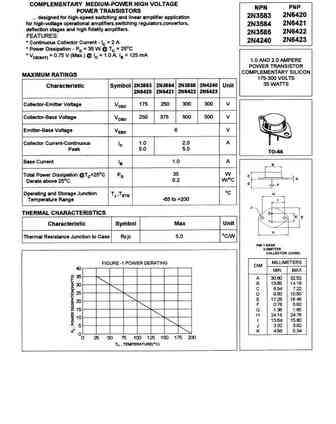
2n6486 2n6487 2n6488 2n6489 2n6490 2n6491.pdf
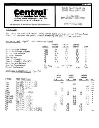
145 Adams Avenue, Hauppauge, NY 11788 USA Tel (631) 435-1110 Fax (631) 435-1824
2n6430 2n6431 2n6432 2n6433.pdf
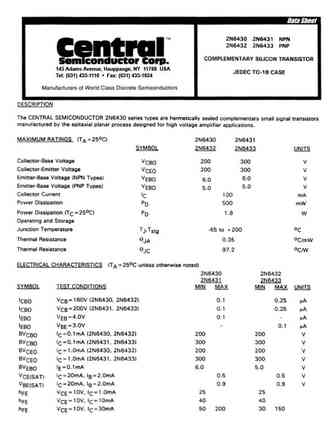
145 Adams Avenue, Hauppauge, NY 11788 USA Tel (631) 435-1110 Fax (631) 435-1824 TM Central Semiconductor Corp. 145 Adams Avenue Hauppauge, NY 11788 USA Tel (631) 435-1110 Fax (631) 435-1824 www.centralsemi.com
2n6473 2n6474 2n6475 2n6476.pdf
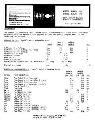
145 Adams Avenue, Hauppauge, NY 11788 USA Tel (631) 435-1110 Fax (631) 435-1824
2n6497-d.pdf
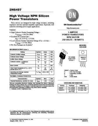
2N6497 High Voltage NPN Silicon Power Transistors These devices are designed for high voltage inverters, switching regulators and line-operated amplifier applications. Especially well suited for switching power supply applications. http //onsemi.com Features 5 AMPERE High Collector-Emitter Sustaining Voltage - VCEO(sus) = 250 Vdc (Min) POWER TRANSISTORS Excellent DC Current
2n6487 2n6488 2n6490 2n6491.pdf
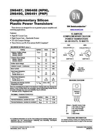
2N6487, 2N6488 (NPN), 2N6490, 2N6491 (PNP) Complementary Silicon Plastic Power Transistors These devices are designed for use in general-purpose amplifier and www.onsemi.com switching applications. Features 15 AMPERE High DC Current Gain COMPLEMENTARY SILICON High Current Gain - Bandwidth Product POWER TRANSISTORS TO-220 Compact Package 60-80 VOLTS, 75 WATTS These
2n6439.pdf
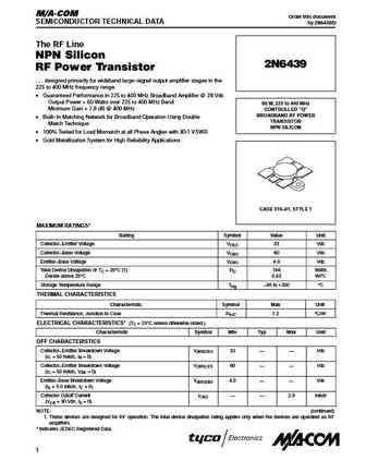
Order this document SEMICONDUCTOR TECHNICAL DATA by 2N6439/D The RF Line NPN Silicon 2N6439 RF Power Transistor . . . designed primarily for wideband large signal output amplifier stages in the 225 to 400 MHz frequency range. Guaranteed Performance in 225 to 400 MHz Broadband Amplifier @ 28 Vdc Output Power = 60 Watts over 225 to 400 MHz Band 60 W, 225 to 400 MHz Minimum Gain
2n6462.pdf

2N6462 Dimensions in mm (inches). Bipolar NPN Device in a 8.51 (0.34) 9.40 (0.37) Hermetically sealed TO39 7.75 (0.305) 8.51 (0.335) Metal Package. 6.10 (0.240) 6.60 (0.260) Bipolar NPN Device. 0.89 max. (0.035) 12.70 (0.500) min. 0.41 (0.016) 0.53 (0.021) VCEO = 300V dia. IC = 0.1A 5.08 (0.200) typ. 2.54 All Semelab hermetically sealed products 2 (0.100) 1
2n6463.pdf

2N6463 Dimensions in mm (inches). Bipolar NPN Device in a 8.51 (0.34) 9.40 (0.37) Hermetically sealed TO39 7.75 (0.305) 8.51 (0.335) Metal Package. 6.10 (0.240) 6.60 (0.260) Bipolar NPN Device. 0.89 max. (0.035) 12.70 (0.500) min. 0.41 (0.016) 0.53 (0.021) VCEO = 250V dia. IC = 0.1A 5.08 (0.200) typ. 2.54 All Semelab hermetically sealed products 2 (0.100) 1
2n6465.pdf

2N6465 Dimensions in mm (inches). Bipolar NPN Device in a Hermetically sealed TO66 6.35 (0.250) Metal Package. 8.64 (0.340) 3.68 (0.145) rad. 3.61 (0.142) max. 4.08(0.161) rad. Bipolar NPN Device. 1 2 VCEO = 110V IC = 4A All Semelab hermetically sealed products can be processed in accordance with the requirements of BS, CECC and JAN, JANTX, JANTXV and JANS speci
2n6466.pdf

2N6466 Dimensions in mm (inches). Bipolar NPN Device in a Hermetically sealed TO66 6.35 (0.250) Metal Package. 8.64 (0.340) 3.68 (0.145) rad. 3.61 (0.142) max. 4.08(0.161) rad. Bipolar NPN Device. 1 2 VCEO = 130V IC = 4A All Semelab hermetically sealed products can be processed in accordance with the requirements of BS, CECC and JAN, JANTX, JANTXV and JANS speci
2n6468.pdf
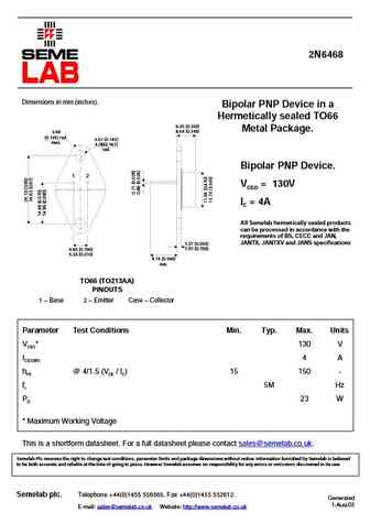
2N6468 Dimensions in mm (inches). Bipolar PNP Device in a Hermetically sealed TO66 6.35 (0.250) Metal Package. 8.64 (0.340) 3.68 (0.145) rad. 3.61 (0.142) max. 4.08(0.161) rad. Bipolar PNP Device. 1 2 VCEO = 130V IC = 4A All Semelab hermetically sealed products can be processed in accordance with the requirements of BS, CECC and JAN, JANTX, JANTXV and JANS speci
2n6425.pdf
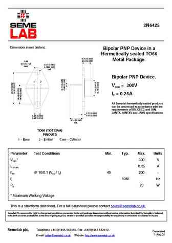
2N6425 Dimensions in mm (inches). Bipolar PNP Device in a Hermetically sealed TO66 6.35 (0.250) Metal Package. 8.64 (0.340) 3.68 (0.145) rad. 3.61 (0.142) max. 4.08(0.161) rad. Bipolar PNP Device. 1 2 VCEO = 300V IC = 0.25A All Semelab hermetically sealed products can be processed in accordance with the requirements of BS, CECC and JAN, JANTX, JANTXV and JANS sp
2n6461.pdf
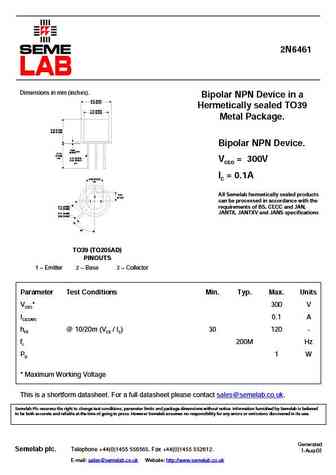
2N6461 Dimensions in mm (inches). Bipolar NPN Device in a 8.51 (0.34) 9.40 (0.37) Hermetically sealed TO39 7.75 (0.305) 8.51 (0.335) Metal Package. 6.10 (0.240) 6.60 (0.260) Bipolar NPN Device. 0.89 max. (0.035) 12.70 (0.500) min. 0.41 (0.016) 0.53 (0.021) VCEO = 300V dia. IC = 0.1A 5.08 (0.200) typ. 2.54 All Semelab hermetically sealed products 2 (0.100) 1
2n6464.pdf

2N6464 Dimensions in mm (inches). Bipolar NPN Device in a 8.51 (0.34) 9.40 (0.37) Hermetically sealed TO39 7.75 (0.305) 8.51 (0.335) Metal Package. 6.10 (0.240) 6.60 (0.260) Bipolar NPN Device. 0.89 max. (0.035) 12.70 (0.500) min. 0.41 (0.016) 0.53 (0.021) VCEO = 250V dia. IC = 0.1A 5.08 (0.200) typ. 2.54 All Semelab hermetically sealed products 2 (0.100) 1
2n6467.pdf

2N6467 Dimensions in mm (inches). Bipolar PNP Device in a Hermetically sealed TO66 6.35 (0.250) Metal Package. 8.64 (0.340) 3.68 (0.145) rad. 3.61 (0.142) max. 4.08(0.161) rad. Bipolar PNP Device. 1 2 VCEO = 110V IC = 4A All Semelab hermetically sealed products can be processed in accordance with the requirements of BS, CECC and JAN, JANTX, JANTXV and JANS speci
2n6497 2n6498 2n6499.pdf
A Boca Semiconductor Corp. (BSC) http //www.bocasemi.com A http //www.bocasemi.com A http //www.bocasemi.com A
2n6436 2n6437 2n6438.pdf
A Boca Semiconductor Corp BSC http //www.bocasemi.com A Boca Semiconductor Corp BSC http //www.bocasemi.com A Boca Semiconductor Corp BSC http //www.bocasemi.com A Boca Semiconductor Corp BSC http //www.bocasemi.com
2n6106 2n6107 2n6108 2n6109 2n6110 2n6111 2n6288 2n6289 2n6290 2n6291 2n6292 2n6293 2n6473 2n6474 2n6475 2n6476.pdf
Boca Semiconductor Corp. BSC http //www.bocasemi.com http //www.bocasemi.com
2n3583 2n3584 2n3585 2n4240 2n6420 2n6421 2n6422 2n6423.pdf
A Boca Semiconductor Corp. http //www.bocasemi.com A http //www.bocasemi.com A http //www.bocasemi.com A http //www.bocasemi.com
2n6494 2n6594.pdf
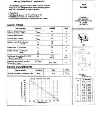
A Boca Semiconductor Corp http //www.bocasemi.com A Boca Semiconductor Corp BSC http //www.bocasemi.com A Boca Semiconductor Corp BSC http //www.bocasemi.com
2n6486-9 2n6490-1.pdf
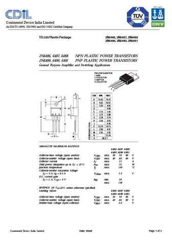
Continental Device India Limited An ISO/TS 16949, ISO 9001 and ISO 14001 Certified Company TO-220 Plastic Package 2N6486, 2N6487, 2N6488 2N6489, 2N6490, 2N6491 2N6486, 6487, 6488 NPN PLASTIC POWER TRANSISTORS 2N6489, 6490, 6491 PNP PLASTIC POWER TRANSISTORS General Purpose Amplifier and Switching Applications PIN CONFIGURATION 4 1. BASE 2. COLLECTOR 3. EMITTER 4. COLLECTOR 1 2 3
2n6430 31.pdf
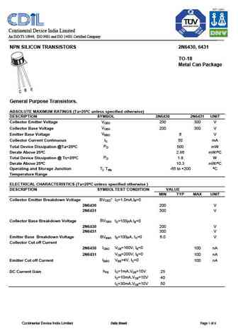
Continental Device India Limited An ISO/TS 16949, ISO 9001 and ISO 14001 Certified Company NPN SILICON TRANSISTORS 2N6430, 6431 TO-18 Metal Can Package General Purpose Transistors. ABSOLUTE MAXIMUM RATINGS (Ta=25 C unless specified otherwise) DESCRIPTION SYMBOL 2N6430 2N6431 UNIT VCEO Collector Emitter Voltage 200 300 V VCBO Collector Base Voltage 200 300 V VEBO Emitter Base Volta
2n6449 2n6450.pdf
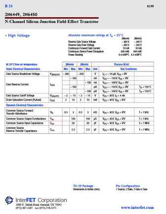
Databook.fxp 1/13/99 2 09 PM Page B-24 B-24 01/99 2N6449, 2N6450 N-Channel Silicon Junction Field-Effect Transistor Absolute maximum ratings at TA = 25 C High Voltage 2N6449 2N6450 Reverse Gate Source Voltage 300 V 200 V Reverse Gate Drain Voltage 300 V 200 V Continuous Forward Gate Current 10 mA 10 mA Continuous Device Power Dissipation 800 mW 800 mW Power Derati
2n6451 2n6452.pdf
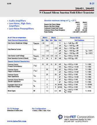
Databook.fxp 1/13/99 2 09 PM Page B-25 01/99 B-25 2N6451, 2N6452 N-Channel Silicon Junction Field-Effect Transistor Absolute maximum ratings at TA = 25 C Audio Amplifiers 2N6451 2N6452 Low-Noise, High Gain Reverse Gate Source Voltage 20 V 25 V Amplifiers Reverse Gate Drain Voltage 20 V 25 V Continuous Forward Gate Current 10 mA 10 mA Low-Noise Preamplifiers
2n6453 2n6454.pdf
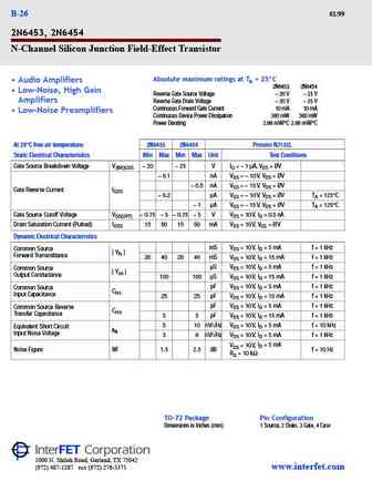
Databook.fxp 1/13/99 2 09 PM Page B-26 B-26 01/99 2N6453, 2N6454 N-Channel Silicon Junction Field-Effect Transistor Absolute maximum ratings at TA = 25 C Audio Amplifiers 2N6453 2N6454 Low-Noise, High Gain Reverse Gate Source Voltage 20 V 25 V Amplifiers Reverse Gate Drain Voltage 20 V 25 V Continuous Forward Gate Current 10 mA 10 mA Low-Noise Preamplifiers
2n6492.pdf
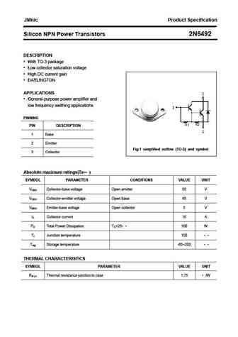
JMnic Product Specification Silicon NPN Power Transistors 2N6492 DESCRIPTION With TO-3 package Low collector saturation voltage High DC current gain DARLINGTON APPLICATIONS General-purpose power amplifier and low frequency swithing applications PINNING PIN DESCRIPTION 1 Base 2 Emitter Fig.1 simplified outline (TO-3) and symbol 3 Collector Absolute maximu
2n6491.pdf

Product Specification www.jmnic.com Silicon PNP Power Transistors 2N6491 DESCRIPTION With TO-220 package Complement to type 2N6488 APPLICATIONS It is intended for use in power linear and low frequency switching applications PINNING PIN DESCRIPTION 1 Base Collector;connected to 2 mounting base 3 Emitter Fig.1 simplified outline (TO-220) and symbol Absolute m
2n6488.pdf

Product Specification www.jmnic.com Silicon NPN Power Transistors 2N6488 DESCRIPTION With TO-220 package Complement to type 2N6491 APPLICATIONS It is intended for use in power linear and low frequency switching applications PINNING PIN DESCRIPTION 1 Base Collector;connected to 2 mounting base 3 Emitter Fig.1 simplified outline (TO-220) and symbol Absolute m
2n6487.pdf

Product Specification www.jmnic.com Silicon NPN Power Transistors 2N6487 DESCRIPTION With TO-220 package Complement to type 2N6490 APPLICATIONS It is intended for use in power linear and low frequency switching applications PINNING PIN DESCRIPTION 1 Base Collector;connected to 2 mounting base 3 Emitter Fig.1 simplified outline (TO-220) and symbol Absolute m
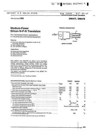
2n6477 2n6478.pdf
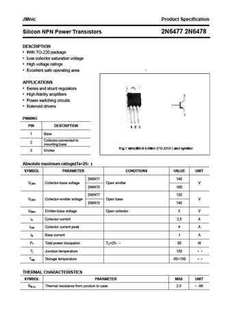
JMnic Product Specification Silicon NPN Power Transistors 2N6477 2N6478 DESCRIPTION With TO-220 package Low collector saturation voltage High voltage ratings Excellent safe operating area APPLICATIONS Series and shunt regulators High-fidelity amplifiers Power switching circuits Solenoid drivers PINNING PIN DESCRIPTION 1 Base Collector;connected to
2n6489 2n6490 2n6491.pdf
JMnic Product Specification Silicon PNP Power Transistors 2N6489 2N6490 2N6491 DESCRIPTION With TO-220 package Excellent safe operating area Complement to type 2N6486 2N6487 2N6488 respectively APPLICATIONS Power amplifier and medium speed switching applications PINNING PIN DESCRIPTION 1 Emitter Collector;connected to 2 mounting base Fig.1 simplified outli
2n6486.pdf
JMnic Product Specification Silicon NPN Power Transistors 2N6486 2N6487 2N6488 DESCRIPTION With TO-220 package Excellent safe operating area Complement to type 2N6489 2N6490 2N6491 respectively APPLICATIONS Power amplifier and medium speed switching applications PINNING PIN DESCRIPTION 1 Base Collector;connected to 2 mounting base 3 Emitter Absolute maxi
2n6420.pdf
JMnic Product Specification Silicon PNP Power Transistors 2N6420 DESCRIPTION With TO-66 package Continuous collector current-IC=-1A Power dissipation -PD=35W @TC=25 Complement to type 2N3583 APPLICATIONS High speed switching and linear amplifier High-voltage operational amplifiers Switching regulators ,converters Deflection stages and high fidelity ampli
2n6490.pdf
Product Specification www.jmnic.com Silicon PNP Power Transistors 2N6490 DESCRIPTION With TO-220 package Complement to type 2N6487 APPLICATIONS It is intended for use in power linear and low frequency switching applications PINNING PIN DESCRIPTION 1 Base Collector;connected to 2 mounting base 3 Emitter Fig.1 simplified outline (TO-220) and symbol Absolute m
2n5419 2n5420 2n5550 2n5551 2n5830 2n5831 2n5832 2n5998 2n5999 2n6008 2n6009 2n6076 2n6426 2n6427.pdf
2n6488.pdf
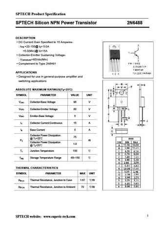
SPTECH Product Specification SPTECH Silicon NPN Power Transistor 2N6488 DESCRIPTION DC Current Gain Specified to 15 Amperes- h =20-150@ I = 5.0A FE C =5.0(Min)@ I =15A C Collector-Emitter Sustaining Voltage- V =80Vdc(Min) CEO(SUS) Complement to Type 2N6491 APPLICATIONS Designed for use in general-purpose amplifier and switching applications ABSOLUTE MAXIMUM RATINGS(T
2n6423.pdf
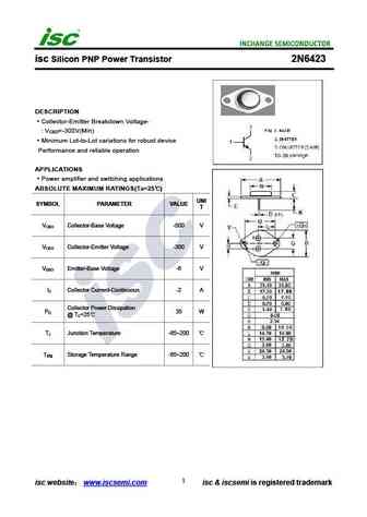
isc Silicon PNP Power Transistor 2N6423 DESCRIPTION Collector-Emitter Breakdown Voltage- V =-300V(Min) CEO Minimum Lot-to-Lot variations for robust device Performance and reliable operation APPLICATIONS Power amplifier and switching applications ABSOLUTE MAXIMUM RATINGS(Ta=25 ) UNI SYMBOL PARAMETER VALUE T V Collector-Base Voltage -500 V CBO V Collector-Emitter Voltage
2n6497 2n6498 2n6499.pdf
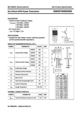
INCHANGE Semiconductor isc Product Specification isc Silicon NPN Power Transistors 2N6497/6498/6499 DESCRIPTION Collector-Emitter Sustaining Voltage- VCEO(SUS)= 250V(Min)- 2N6497 = 300V(Min)- 2N6498 = 350V(Min)- 2N6499 DC Current Gain- hFE= 10-75@IC= 2.5A APPLICATIONS Designed for high voltage inverters, switching regulators and line operated amplifier applica
2n6470 2n6471 2n6472.pdf
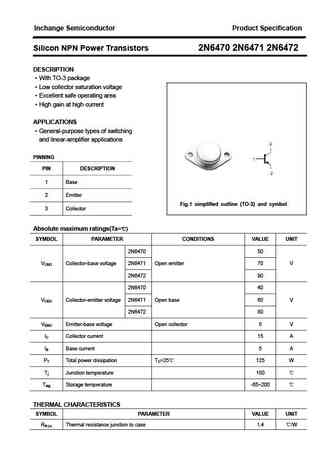
Inchange Semiconductor Product Specification Silicon NPN Power Transistors 2N6470 2N6471 2N6472 DESCRIPTION With TO-3 package Low collector saturation voltage Excellent safe operating area High gain at high current APPLICATIONS General-purpose types of switching and linear-amplifier applications PINNING PIN DESCRIPTION 1 Base 2 Emitter Fig.1 simplified outlin
2n6492.pdf

isc Silicon NPN Darlington Power Transistor 2N6492 DESCRIPTION High DC current gain h = 500(Min)@ I = 3A FE C With TO-3 package Low collector saturation 100% avalanche tested Minimum Lot-to-Lot variations for robust device performance and reliable operation APPLICATIONS Designed for general-purpose power amplifier and low frequency swithing applications. ABSOLUTE MAXI
2n6495.pdf
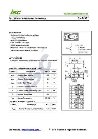
isc Silicon NPN Power Transistor 2N6495 DESCRIPTION Collector-Emitter Sustaining Voltage- V = 80V(Min.) CEO With TO-66 package Low collector saturation 100% avalanche tested Minimum Lot-to-Lot variations for robust device performance and reliable operation APPLICATIONS Designed for switching and wide-band amplifier applications. ABSOLUTE MAXIMUM RATINGS(T =25 ) a S
2n6425.pdf

isc Silicon PNP Power Transistor 2N6425 DESCRIPTION Collector-Emitter Breakdown Voltage- V =-300V(Min) CEO Minimum Lot-to-Lot variations for robust device Performance and reliable operation APPLICATIONS Power amplifier and switching applications ABSOLUTE MAXIMUM RATINGS(Ta=25 ) UNI SYMBOL PARAMETER VALUE T V Collector-Base Voltage -325 V CBO V Collector-Emitter Voltage
2n6488.pdf
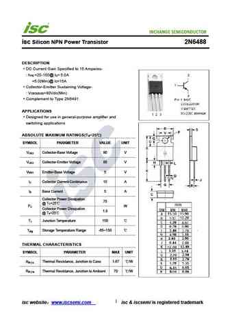
INCHANGE Semiconductor isc Silicon NPN Power Transistor 2N6488 DESCRIPTION DC Current Gain Specified to 15 Amperes- h =20-150@ I = 5.0A FE C =5.0(Min)@ I =15A C Collector-Emitter Sustaining Voltage- V =80Vdc(Min) CEO(SUS) Complement to Type 2N6491 APPLICATIONS Designed for use in general-purpose amplifier and switching applications ABSOLUTE MAXIMUM RATINGS(T =25 )
2n6486 2n6487 2n6488.pdf
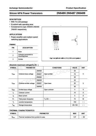
Inchange Semiconductor Product Specification Silicon NPN Power Transistors 2N6486 2N6487 2N6488 DESCRIPTION With TO-220 package Excellent safe operating area Complement to type 2N6489 2N6490 2N6491 respectively APPLICATIONS Power amplifier and medium speed switching applications PINNING PIN DESCRIPTION 1 Base Collector;connected to 2 mounting base 3 Emitte
2n6467 2n6468.pdf
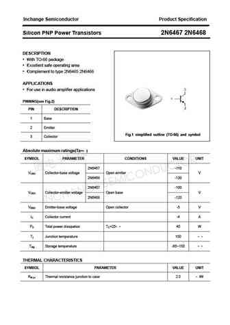
Inchange Semiconductor Product Specification Silicon PNP Power Transistors 2N6467 2N6468 DESCRIPTION With TO-66 package Excellent safe operating area Complement to type 2N6465 2N6466 APPLICATIONS For use in audio amplifier applications PINNING(see Fig.2) PIN DESCRIPTION 1 Base 2 Emitter Fig.1 simplified outline (TO-66) and symbol 3 Collector Absolute maximum rati
2n6493.pdf
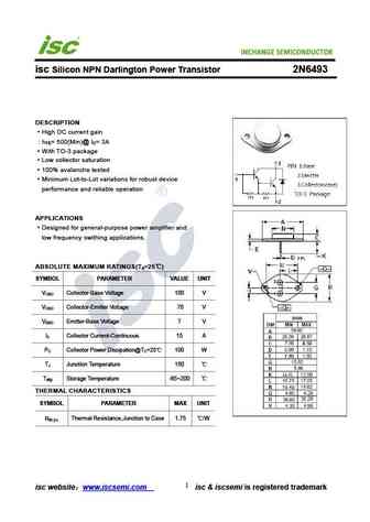
isc Silicon NPN Darlington Power Transistor 2N6493 DESCRIPTION High DC current gain h = 500(Min)@ I = 3A FE C With TO-3 package Low collector saturation 100% avalanche tested Minimum Lot-to-Lot variations for robust device performance and reliable operation APPLICATIONS Designed for general-purpose power amplifier and low frequency swithing applications. ABSOLUTE MAXI
2n6475 2n6476.pdf
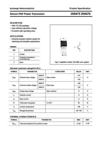
Inchange Semiconductor Product Specification Silicon PNP Power Transistors 2N6475 2N6476 DESCRIPTION With TO-220 package Low collector saturation voltage Excellent safe operating area APPLICATIONS General-purpose medium power for switching and amplifier applications PINNING PIN DESCRIPTION 1 Emitter Collector;connected to 2 mounting base Fig.1 simplified out
2n6470.pdf

INCHANGE Semiconductor isc Product Specification isc Silicon NPN Power Transistor 2N6470 DESCRIPTION Excellent Safe Operating Area High DC Current Gain- hFE= 20-150(Min)@IC = 5A Low Saturation Voltage- VCE(sat)= 1.3V(Max)@ IC = 5A APPLICATIONS Designed for general-purpose switching and linear amplifier applications. ABSOLUTE MAXIMUM RATINGS(Ta=25 ) SYMBOL
2n6477 2n6478.pdf
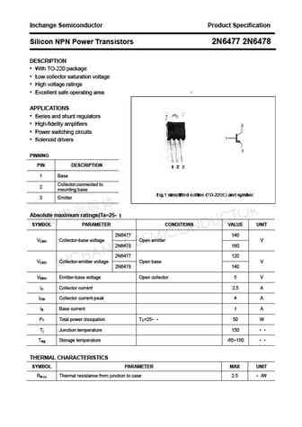
Inchange Semiconductor Product Specification Silicon NPN Power Transistors 2N6477 2N6478 DESCRIPTION With TO-220 package Low collector saturation voltage High voltage ratings Excellent safe operating area APPLICATIONS Series and shunt regulators High-fidelity amplifiers Power switching circuits Solenoid drivers PINNING PIN DESCRIPTION 1 Base Collecto
2n6436 2n6437 2n6438.pdf
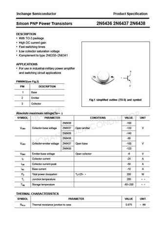
Inchange Semiconductor Product Specification Silicon PNP Power Transistors 2N6436 2N6437 2N6438 DESCRIPTION With TO-3 package High DC current gain Fast switching times Low collector saturation voltage Complement to type 2N6338 2N6341 APPLICATIONS For use in industrial-military power amplifier and switching circuit applications PINNING(see Fig.2) PIN DESCRIPT
2n6489 2n6490 2n6491.pdf
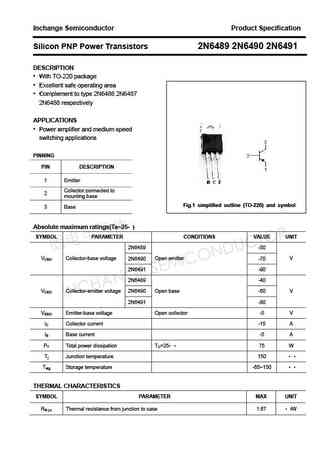
Inchange Semiconductor Product Specification Silicon PNP Power Transistors 2N6489 2N6490 2N6491 DESCRIPTION With TO-220 package Excellent safe operating area Complement to type 2N6486 2N6487 2N6488 respectively APPLICATIONS Power amplifier and medium speed switching applications PINNING PIN DESCRIPTION 1 Emitter Collector;connected to 2 mounting base Fig.1
2n6494.pdf

isc Silicon NPN Darlington Power Transistor 2N6494 DESCRIPTION High DC current gain h = 500(Min)@ I = 3A FE C With TO-3 package Low collector saturation 100% avalanche tested Minimum Lot-to-Lot variations for robust device performance and reliable operation APPLICATIONS Designed for general-purpose power amplifier and low frequency swithing applications. ABSOLUTE MAXI
2n6469.pdf
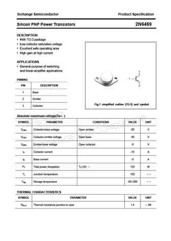
Inchange Semiconductor Product Specification Silicon PNP Power Transistors 2N6469 DESCRIPTION With TO-3 package Low collector saturation voltage Excellent safe operating area High gain at high current APPLICATIONS General-purpose of switching and linear-amplifier applications PINNING PIN DESCRIPTION 1 Base 2 Emitter Fig.1 simplified outline (TO-3) and symbol
2n6422.pdf

isc Silicon PNP Power Transistor 2N6422 DESCRIPTION Collector-Emitter Breakdown Voltage- V =-300V(Min) CEO Minimum Lot-to-Lot variations for robust device Performance and reliable operation APPLICATIONS Power amplifier and switching applications ABSOLUTE MAXIMUM RATINGS(Ta=25 ) UNI SYMBOL PARAMETER VALUE T V Collector-Base Voltage -500 V CBO V Collector-Emitter Voltage
2n6465 2n6466.pdf

Inchange Semiconductor Product Specification Silicon NPN Power Transistors 2N6465 2N6466 DESCRIPTION With TO-66 package Excellent safe operating area Complement to type 2N6467 2N6468 APPLICATIONS For use in audio amplifier applications PINNING(see Fig.2) PIN DESCRIPTION 1 Base 2 Emitter Fig.1 simplified outline (TO-66) and symbol 3 Collector Absolute maximum rat
2n6473 2n6474.pdf
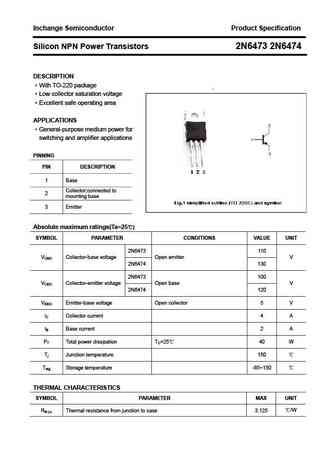
Inchange Semiconductor Product Specification Silicon NPN Power Transistors 2N6473 2N6474 DESCRIPTION With TO-220 package Low collector saturation voltage Excellent safe operating area APPLICATIONS General-purpose medium power for switching and amplifier applications PINNING PIN DESCRIPTION 1 Base Collector;connected to 2 mounting base 3 Emitter Absolute ma
2n6420.pdf
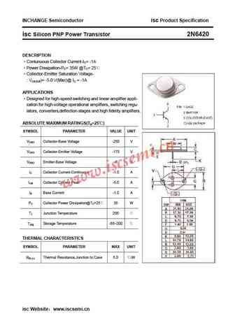
INCHANGE Semiconductor isc Product Specification isc Silicon PNP Power Transistor 2N6420 DESCRIPTION Contunuous Collector Current-IC= -1A Power Dissipation-PC= 35W @TC= 25 Collector-Emitter Saturation Voltage- VCE(sat)= -5.0 V(Max)@ IC = -1A APPLICATIONS Designed for high-speed switching and linear amplifier appli- cation for high-voltage operational amplifiers, s
Otros transistores... 2N638B , 2N639 , 2N6390 , 2N6391 , 2N6392 , 2N6393 , 2N639A , 2N639B , 2N2907 , 2N640 , 2N6406 , 2N6407 , 2N6408 , 2N6409 , 2N641 , 2N6410 , 2N6411 .
History: 2N6602 | 2SD1377
🌐 : EN ES РУ

Liste
Recientemente añadidas las descripciónes de los transistores:
BJT: GA1A4M | SBT42 | 2SA200-Y | 2SA200-O | 2SD882-Q | 2SD882-P | 2SD882-E | 2SC945-L | 2SC945-H | 2SC4226-R23 | 2SC3357-F | 2SC3357-E | 2SC3356-R26 | 2SC3356-R24 | 2SC3356-R23 | 2SB772-Q | 2SB772-P | 2SB772-E | 2SA1015-L | 2SA1015-H | HSS8550
Popular searches
2n5551 | irf540n | irf3205 mosfet | 2n3055 | irfp260n | 2n2222 datasheet | irf9540 | 2n3055 datasheet