MP4013 Datasheet. Equivalente. Reemplazo. Hoja de especificaciones. Principales características
Número de Parte: MP4013 📄📄
Material: Si
Polaridad de transistor: NPN
ESPECIFICACIONES MÁXIMAS
Disipación total del dispositivo (Pc): 2 W
Tensión colector-base (Vcb): 80 V
Tensión colector-emisor (Vce): 80 V
Tensión emisor-base (Veb): 8 V
Corriente del colector DC máxima (Ic): 2 A
Temperatura operativa máxima (Tj): 150 °C
CARACTERÍSTICAS ELÉCTRICAS
Transición de frecuencia (fT): 100 MHz
Capacitancia de salida (Cc): 20 pF
Ganancia de corriente contínua (hFE): 2000
Encapsulados: 2-25A1A
📄📄 Copiar
Búsqueda de reemplazo de MP4013
- Selecciónⓘ de transistores por parámetros
MP4013 datasheet
..1. Size:126K toshiba
mp4013.pdf 
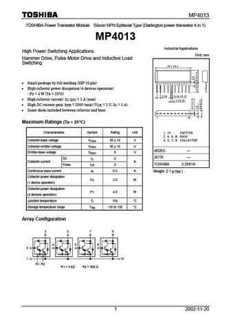
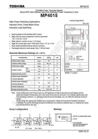
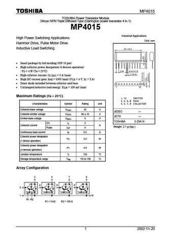
MP4013 TOSHIBA Power Transistor Module Silicon NPN Epitaxial Type (Darlington power transistor 4 in 1) MP4013 Industrial Applications High Power Switching Applications. Unit mm Hammer Drive, Pulse Motor Drive and Inductive Load Switching. Small package by full molding (SIP 10 pin) High collector power dissipation (4 devices operation) P = 4 W (Ta = 25 C) T
..2. Size:167K toshiba
mp4013 .pdf
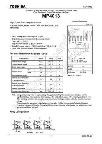
MP4013 TOSHIBA Power Transistor Module Silicon NPN Epitaxial Type (Four Darlington Power Transistors 4 in One) MP4013 Industrial Applications High Power Switching Applications Unit mm Hammer Drive, Pulse Motor Drive and Inductive Load Switching Small package by full molding (SIP 10 pins) High collector power dissipation (4-device operation) PT = 4 W (Ta = 25 C)
0.1. Size:516K diodes
dmp4013lfg.pdf
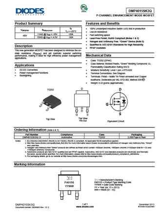
DMP4013LFG 40V P-CHANNEL ENHANCEMENT MODE MOSFET POWERDI Product Summary Features and Benefits Low RDS(ON) ensures on state losses are minimized. ID max BVDSS RDS(ON) max Small form factor thermally efficient package enables higher TA = +25 C 13m @ VGS = -10V -10.3A density end products. -40V 18m @ VGS = -4.5V -8.8A Occupies 33% of the board area
0.2. Size:603K diodes
dmp4013lfgq.pdf
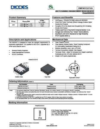
DMP4013LFGQ 40V P-CHANNEL ENHANCEMENT MODE MOSFET PowerDI3333-8 Product Summary Features and Benefits Low RDS(ON) Ensures On-State Losses are Minimized ID Max BVDSS RDS(ON) Max Small Form Factor Thermally Efficient Package Enables Higher TA = +25 C 13m @ VGS = -10V -10.3A Density End Products -40V 18m @ VGS = -4.5V -8.8A Occupies 33% of the Board
9.1. Size:359K 1
dmp4015sps-13.pdf
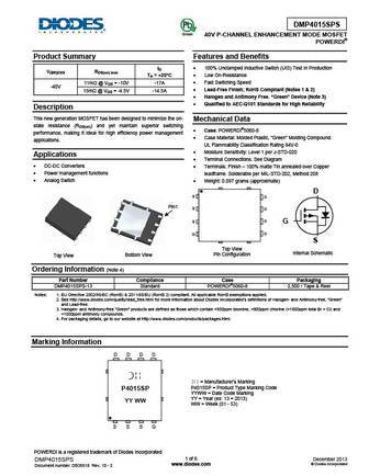
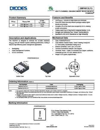
DMP4015SPS Green 40V P-CHANNEL ENHANCEMENT MODE MOSFET POWERDI Product Summary Features and Benefits 100% Unclamped Inductive Switch (UIS) Test In Production ID V(BR)DSS RDS(on) max TA = +25 C Low On-Resistance Fast Switching Speed 11m @ VGS = -10V -17A -40V Lead-Free Finish; RoHS Compliant (Notes 1 & 2) 15m @ VGS = -4.5V -14.5A Halogen and
9.2. Size:177K toshiba
mp4015 .pdf
MP4015 TOSHIBA Power Transistor Module Silicon NPN Triple Diffused Type (Four Darlington Power Transistors in One) MP4015 Industrial Applications High Power Switching Applications Unit mm Hammer Drive, Pulse Motor Drive Inductive Load Switching Small package by full molding (SIP 10 pins) High collector power dissipation (4-device operation) PT = 4 W (Ta = 25 C)
9.3. Size:130K toshiba
mp4015.pdf
MP4015 TOSHIBA Power Transistor Module Silicon NPN Triple Diffused Type (Darlington power transistor 4 in 1) MP4015 Industrial Applications High Power Switching Applications. Unit mm Hammer Drive, Pulse Motor Drive. Inductive Load Switching. Small package by full molding (SIP 10 pin) High collector power dissipation (4 devices operation) P = 4 W (Ta = 25 C) T
9.4. Size:363K diodes
dmp4015spsq.pdf
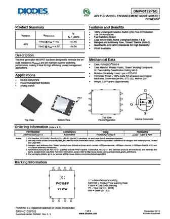
DMP4015SPSQ Green 40V P-CHANNEL ENHANCEMENT MODE MOSFET POWERDI Product Summary Features and Benefits 100% Unclamped Inductive Switch (UIS) Test In Production ID Low On-Resistance V(BR)DSS RDS(on) max TA = +25 C Fast Switching Speed Lead-Free Finish; RoHS Compliant (Notes 1 & 2) 11m @ VGS = -10V -17.0A Halogen and Antimony Free. Green Device
9.5. Size:270K diodes
dmp4015sssq.pdf
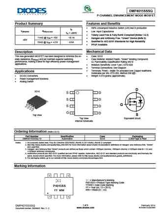
DMP4015SSSQ P-CHANNEL ENHANCEMENT MODE MOSFET Product Summary Features and Benefits 100% Unclamped Inductive Switch (UIS) test in production ID V(BR)DSS RDS(on) max Low Input Capacitance TA = +25 C Totally Lead-Free & Fully RoHS Compliant (Notes 1 & 2) 11m @ VGS = -10V -10.1A Halogen and Antimony Free. Green Device (Note 3) -40V Qualified to
9.6. Size:202K diodes
dmp4015sps.pdf
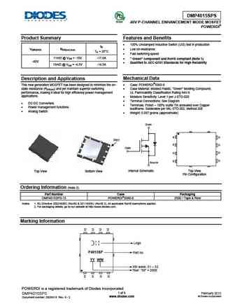
DMP4015SPS Green 40V P-CHANNEL ENHANCEMENT MODE MOSFET POWERDI Product Summary Features and Benefits 100% Unclamped Inductive Switch (UIS) test in production ID V(BR)DSS RDS(on) max Low on-resistance TA = 25 C Fast switching speed 11m @ VGS = -10V -17.0A " Green component and RoHS compliant (Note 1) -40V Qualified to AEC-Q101 Standards for Hig
9.7. Size:224K diodes
dmp4015sk3.pdf
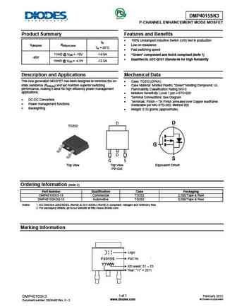
DMP4015SK3 P-CHANNEL ENHANCEMENT MODE MOSFET Product Summary Features and Benefits 100% Unclamped Inductive Switch (UIS) test in production ID V(BR)DSS RDS(on) max Low on-resistance TA = 25 C Fast switching speed 11m @ VGS = -10V -14.0A Green component and RoHS compliant (Note 1) -40V Qualified to AEC-Q101 Standards for High Reliability 15m
9.9. Size:189K diodes
dmp4015sss.pdf
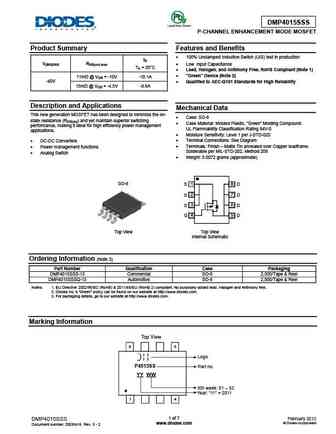
DMP4015SSS P-CHANNEL ENHANCEMENT MODE MOSFET Product Summary Features and Benefits 100% Unclamped Inductive Switch (UIS) test in production ID V(BR)DSS RDS(on) max Low Input Capacitance TA = 25 C Lead, Halogen, and Antimony Free, RoHS Compliant (Note 1) "Green" Device (Note 2) 11m @ VGS = -10V -10.1A -40V Qualified to AEC-Q101 Standards for High Rel
9.10. Size:1482K cn vbsemi
dmp4015sssq.pdf
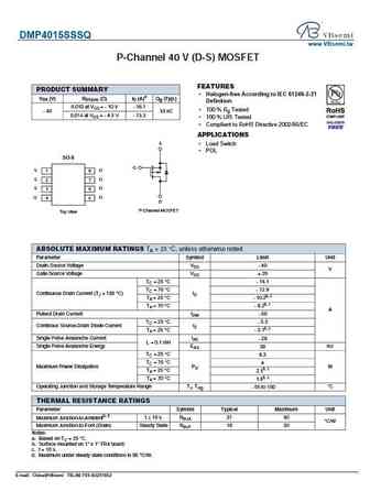
DMP4015SSSQ www.VBsemi.tw P-Channel 40 V (D-S) MOSFET FEATURES PRODUCT SUMMARY Halogen-free According to IEC 61249-2-21 VDS (V) RDS(on) ( )ID (A)a Qg (Typ.) Definition 0.010 at VGS = - 10 V - 16.1 100 % Rg Tested - 40 33 nC 0.014 at VGS = - 4.5 V - 13.3 100 % UIS Tested Compliant to RoHS Directive 2002/95/EC APPLICATIONS S Load Switch POL SO-8 G SD
9.11. Size:266K inchange semiconductor
dmp4015sk3.pdf
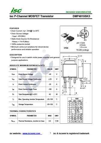
isc P-Channel MOSFET Transistor DMP4015SK3 FEATURES Drain Current I = -35A@ T =25 D C Drain Source Voltage- V = -40V(Min) DSS Static Drain-Source On-Resistance R = 11m (Max) DS(on) 100% avalanche tested Minimum Lot-to-Lot variations for robust device performance and reliable operation DESCRIPTION Designed for use in switch mode power supplies and general pu
Otros transistores... MT6L04AE, MT6L71FS, MT6L76FS, MT6L77FS, MT6L78FS, MP4005, MP4006, MP4009, 2SD669, MP4015, MP4020, MP4021, MP4024, MP4025, MP4101, MP4104, MP42001