DD05 Equivalente. Reemplazo. Hoja de especificaciones. Principales características
Número de Parte: DD05
Material: Si
Polaridad de transistor: NPN
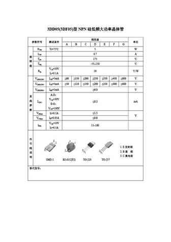
ESPECIFICACIONES MÁXIMAS
Disipación total del dispositivo (Pc): 30 W
Tensión colector-emisor (Vce): 60 V
Tensión emisor-base (Veb): 5 V
Corriente del colector DC máxima (Ic): 6 A
Temperatura operativa máxima (Tj): 175 °C
CARACTERÍSTICAS ELÉCTRICAS
Ganancia de corriente contínua (hFE): 70
Encapsulados: TO-3
Búsqueda de reemplazo de DD05
- Selecciónⓘ de transistores por parámetros
DD05 datasheet
dd05.pdf
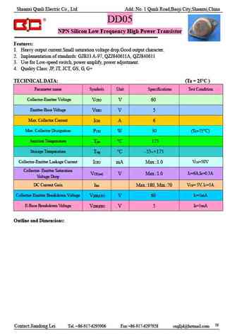
Shaanxi Qunli Electric Co., Ltd Add. No. 1 Qunli Road,Baoji City,Shaanxi,China DD05 NPN Silicon Low Frequency High Power Transistor Features 1. Heavy output current.Small saturation voltage drop.Good output character. 2. Implementation of standards GJB33 A-97, QZJ840611A, QZJ840611 3. Use for Low-speed switch, power amplify, power adjustment. 4. Quality Class JP, JT, JCT, GS, G,
fdd050n03b.pdf
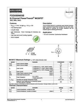
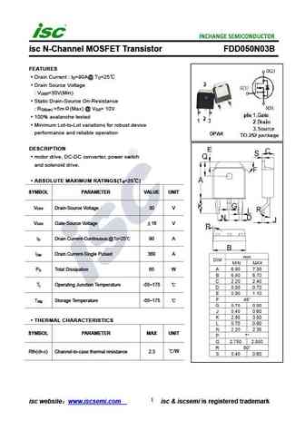
March 2010 FDD050N03B N-Channel PowerTrench MOSFET 30V, 90A, 5m Features Description RDS(on) = 3.7m ( Typ.)@ VGS = 10V, ID = 25A This N-Channel MOSFET is produced using Fairchild Semicon- ductor s advanced PowerTrench process that has been espe- Fast Switching Speed cially tailored to minimize the on-state resistance and yet maintain superior switching performance.
rdd050n20.pdf
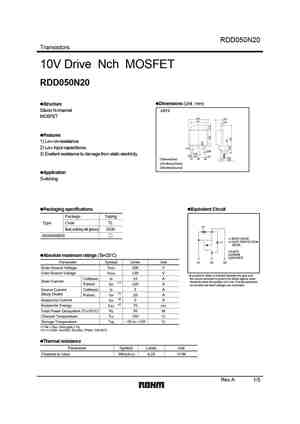
RDD050N20 Transistors 10V Drive Nch MOSFET RDD050N20 Dimensions (Unit mm) Structure Silicon N-channel CPT3 MOSFET Features 1) Low on-resistance. 2) Low input capacitance. 3) Exellent resistance to damage from static electricity. (1)Base(Gate) (2)Collector(Drain) (3)Emitter(Source) Application Switching Packaging specifications Equivalent Circuit Package
ndf05n50z ndp05n50z ndd05n50z.pdf
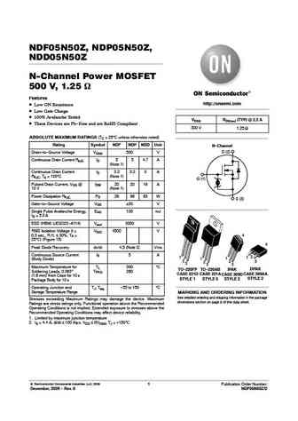
NDF05N50Z, NDP05N50Z, NDD05N50Z N-Channel Power MOSFET 500 V, 1.25 W Features http //onsemi.com Low ON Resistance Low Gate Charge 100% Avalanche Tested VDSS RDS(on) (TYP) @ 2.2 A These Devices are Pb-Free and are RoHS Compliant 500 V 1.25 W ABSOLUTE MAXIMUM RATINGS (TC = 25 C unless otherwise noted) Rating Symbol NDF NDP NDD Unit N-Channel D (2) Drain-to-Source


Otros transistores... CHUMF24GP, CHUMF4GP, CHUMF5GP, CHUMF7GP, CHUMF8GP, DD03T, DD04, DD04T, 2SC5198, DD05T, DMA50101, DMA50201, DMA50401, DMA50601, DMA50601, DMBT2222, DMBT2222A
🌐 : EN ES РУ

Liste
Recientemente añadidas las descripciónes de los transistores:
BJT: GA1A4M | SBT42 | 2SA200-Y | 2SA200-O | 2SD882-Q | 2SD882-P | 2SD882-E | 2SC945-L | 2SC945-H | 2SC4226-R23 | 2SC3357-F | 2SC3357-E | 2SC3356-R26 | 2SC3356-R24 | 2SC3356-R23 | 2SB772-Q | 2SB772-P | 2SB772-E | 2SA1015-L | 2SA1015-H | HSS8550
Popular searches
2sc793 | 2sd313 replacement | 2n4249 | a1013 transistor | 2sc2705 | bc239 | 2sc3264 | mp38a