DD05 Specs and Replacement
Type Designator: DD05
Material of Transistor: Si
Polarity: NPN
Absolute Maximum Ratings
Maximum Collector Power Dissipation (Pc): 30 W
Maximum Collector-Emitter Voltage |Vce|: 60 V
Maximum Emitter-Base Voltage |Veb|: 5 V
Maximum Collector Current |Ic max|: 6 A
Max. Operating Junction Temperature (Tj): 175 °C
Electrical Characteristics
Forward Current Transfer Ratio (hFE), MIN: 70
Noise Figure, dB: -
Package: TO-3
- BJT ⓘ Cross-Reference Search
DD05 datasheet
..1. Size:23K shaanxi
dd05.pdf 

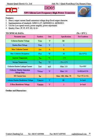
Shaanxi Qunli Electric Co., Ltd Add. No. 1 Qunli Road,Baoji City,Shaanxi,China DD05 NPN Silicon Low Frequency High Power Transistor Features 1. Heavy output current.Small saturation voltage drop.Good output character. 2. Implementation of standards GJB33 A-97, QZJ840611A, QZJ840611 3. Use for Low-speed switch, power amplify, power adjustment. 4. Quality Class JP, JT, JCT, GS, G,... See More ⇒
0.1. Size:717K fairchild semi
fdd050n03b.pdf 

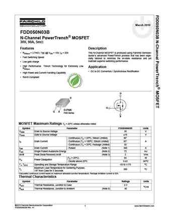
March 2010 FDD050N03B N-Channel PowerTrench MOSFET 30V, 90A, 5m Features Description RDS(on) = 3.7m ( Typ.)@ VGS = 10V, ID = 25A This N-Channel MOSFET is produced using Fairchild Semicon- ductor s advanced PowerTrench process that has been espe- Fast Switching Speed cially tailored to minimize the on-state resistance and yet maintain superior switching performance. ... See More ⇒
0.2. Size:157K rohm
rdd050n20.pdf 

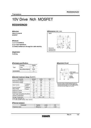
RDD050N20 Transistors 10V Drive Nch MOSFET RDD050N20 Dimensions (Unit mm) Structure Silicon N-channel CPT3 MOSFET Features 1) Low on-resistance. 2) Low input capacitance. 3) Exellent resistance to damage from static electricity. (1)Base(Gate) (2)Collector(Drain) (3)Emitter(Source) Application Switching Packaging specifications Equivalent Circuit Package... See More ⇒
0.3. Size:157K onsemi
ndf05n50z ndp05n50z ndd05n50z.pdf 

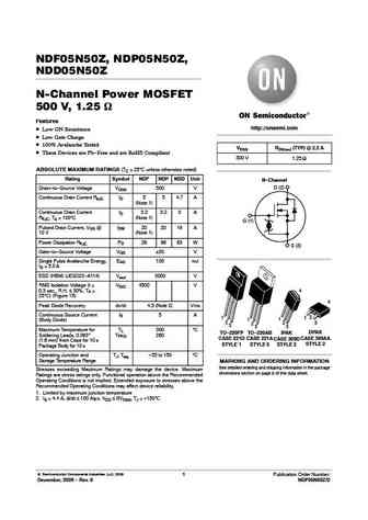
NDF05N50Z, NDP05N50Z, NDD05N50Z N-Channel Power MOSFET 500 V, 1.25 W Features http //onsemi.com Low ON Resistance Low Gate Charge 100% Avalanche Tested VDSS RDS(on) (TYP) @ 2.2 A These Devices are Pb-Free and are RoHS Compliant 500 V 1.25 W ABSOLUTE MAXIMUM RATINGS (TC = 25 C unless otherwise noted) Rating Symbol NDF NDP NDD Unit N-Channel D (2) Drain-to-Source... See More ⇒
0.4. Size:570K onsemi
fdd050n03b.pdf 

Is Now Part of To learn more about ON Semiconductor, please visit our website at www.onsemi.com Please note As part of the Fairchild Semiconductor integration, some of the Fairchild orderable part numbers will need to change in order to meet ON Semiconductor s system requirements. Since the ON Semiconductor product management systems do not have the ability to manage part nomenclatur... See More ⇒
0.5. Size:159K samhop
sdu05n04 sdd05n04.pdf 

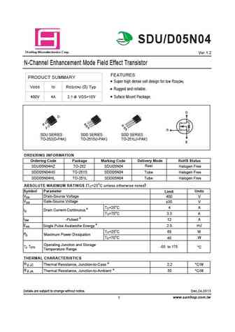
Green Product SDU/D05N04 a S mHop Microelectronics C orp. Ver 1.2 N-Channel Enhancement Mode Field Effect Transistor FEATURES PRODUCT SUMMARY Super high dense cell design for low RDS(ON). VDSS ID RDS(ON) ( ) Typ Rugged and reliable. 400V 4A 2.1 @ VGS=10V Suface Mount Package. D G S SDU SERIES SDD SERIES SDD SERIES TO-252(D-PAK) TO-251S(I-PAK) TO-251L(I-PAK) ORDERING INFORMATI... See More ⇒
0.6. Size:156K samhop
sdu05n70 sdd05n70.pdf 

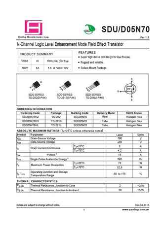
Green Product SDU/D05N70 a S mHop Microelectronics C orp. Ver 1.1 N-Channel Logic Level Enhancement Mode Field Effect Transistor FEATURES PRODUCT SUMMARY Super high dense cell design for low RDS(ON). VDSS ID RDS(ON) ( ) Typ Rugged and reliable. 700V 5A 1.6 @ VGS=10V Suface Mount Package. D G S SDU SERIES SDD SERIES SDD SERIES TO-252(D-PAK) TO-251S(I-PAK) TO-251L(I-PAK) ORDERIN... See More ⇒
0.7. Size:149K china
3dd05.pdf 

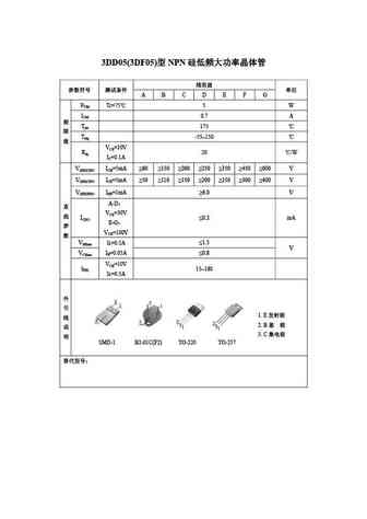
3DD05(3DF05) NPN A B C D E F G PCM Tc=75 5 W ICM 0.7 A Tjm 175 Tstg -55 150 VCE=10V Rth 20 /W IC=0.1A V(BR)CBO ICB=5mA 80 150 200 250 350 450 600 V V(BR)CEO ICE=5mA 50 110 150 200 250 300 400 V V(BR)EBO IEB=1mA 6.0 V A-D... See More ⇒
0.8. Size:144K china
3dd05t.pdf 

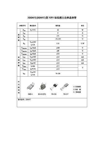
3DD05T(DD05T) NPN PCM TC=75 30 W ICM 6 A Tjm 175 Tstg -55 150 VCE=10V Rth 3.33 /W IC=1A V(BR)CBO ICB=2mA 100 V V(BR)CEO ICE=2mA 60 V V(BR)EBO IEB=2mA 5.0 V ICBO VCB=50V 1.0 mA ICEO VCE=50V 1.0 mA IEBO VEB=4V 1.0 mA VBEsat ... See More ⇒
0.9. Size:144K china
dd05t.pdf 

3DD05T(DD05T) NPN PCM TC=75 30 W ICM 6 A Tjm 175 Tstg -55 150 VCE=10V Rth 3.33 /W IC=1A V(BR)CBO ICB=2mA 100 V V(BR)CEO ICE=2mA 60 V V(BR)EBO IEB=2mA 5.0 V ICBO VCB=50V 1.0 mA ICEO VCE=50V 1.0 mA IEBO VEB=4V 1.0 mA VBEsat ... See More ⇒
0.10. Size:308K inchange semiconductor
fdd050n03b.pdf 
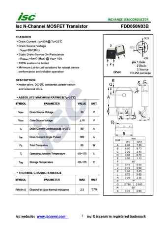
isc N-Channel MOSFET Transistor FDD050N03B FEATURES Drain Current I =90A@ T =25 D C Drain Source Voltage V =30V(Min) DSS Static Drain-Source On-Resistance R =5m (Max) @ V = 10V DS(on) GS 100% avalanche tested Minimum Lot-to-Lot variations for robust device performance and reliable operation DESCRIPTION motor drive, DC-DC converter, power switch and solenoid ... See More ⇒
Detailed specifications: CHUMF24GP, CHUMF4GP, CHUMF5GP, CHUMF7GP, CHUMF8GP, DD03T, DD04, DD04T, 2SC5198, DD05T, DMA50101, DMA50201, DMA50401, DMA50601, DMA50601, DMBT2222, DMBT2222A
Keywords - DD05 pdf specs
DD05 cross reference
DD05 equivalent finder
DD05 pdf lookup
DD05 substitution
DD05 replacement
![]()
