APT20M45SVFR Specs and Replacement
Type Designator: APT20M45SVFR
Type of Transistor: MOSFET
Type of Control Channel: N-Channel
Absolute Maximum Ratings
Pd ⓘ - Maximum Power Dissipation: 300 W
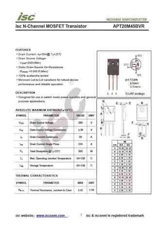
|Vds|ⓘ - Maximum Drain-Source Voltage: 200 V
|Vgs|ⓘ - Maximum Gate-Source Voltage: 30 V
|Id| ⓘ - Maximum Drain Current: 56 A
Tj ⓘ - Maximum Junction Temperature: 150 °C
Electrical Characteristics
tr ⓘ - Rise Time: 14 nS
Cossⓘ - Output Capacitance: 980 pF
RDSonⓘ - Maximum Drain-Source On-State Resistance: 0.045 Ohm
Package: D3PAK
APT20M45SVFR substitution
- MOSFET ⓘ Cross-Reference Search
APT20M45SVFR datasheet
apt20m45svfr.pdf
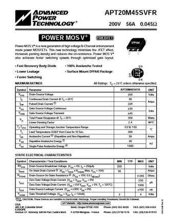
APT20M45SVFR 200V 56A 0.045 POWER MOS V FREDFET D3PAK Power MOS V is a new generation of high voltage N-Channel enhancement mode power MOSFETs. This new technology minimizes the JFET effect, increases packing density and reduces the on-resistance. Power MOS V also achieves faster switching speeds through optimized gate layout. Fast Recovery Body Diode 100% Avalanche Tes... See More ⇒
apt20m45svr.pdf
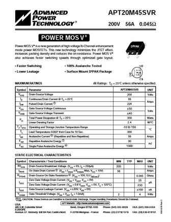
APT20M45SVR 200V 56A 0.045 POWER MOS V Power MOS V is a new generation of high voltage N-Channel enhancement D3PAK mode power MOSFETs. This new technology minimizes the JFET effect, increases packing density and reduces the on-resistance. Power MOS V also achieves faster switching speeds through optimized gate layout. Faster Switching 100% Avalanche Tested D Lower L... See More ⇒
apt20m45bvr.pdf
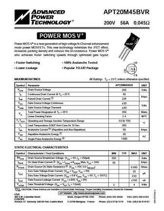
APT20M45BVR 200V 56A 0.045 POWER MOS V Power MOS V is a new generation of high voltage N-Channel enhancement TO-247 mode power MOSFETs. This new technology minimizes the JFET effect, increases packing density and reduces the on-resistance. Power MOS V also achieves faster switching speeds through optimized gate layout. Faster Switching 100% Avalanche Tested D Lower ... See More ⇒
apt20m45bvfr.pdf
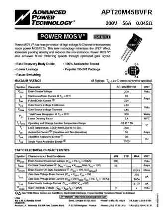
APT20M45BVFR 200V 56A 0.045 POWER MOS V FREDFET Power MOS V is a new generation of high voltage N-Channel enhancement TO-247 mode power MOSFETs. This new technology minimizes the JFET effect, increases packing density and reduces the on-resistance. Power MOS V also achieves faster switching speeds through optimized gate layout. Fast Recovery Body Diode 100% Avalanche Tes... See More ⇒

Detailed specifications: APT20M26WVR, APT20M38BVFR, APT20M38BVR, APT20M38SVR, APT20M40BVR, APT20M42HVR, APT20M45BVFR, APT20M45BVR, IRF840, APT20M45SVR, APT30M19JVFR, APT30M19JVR, APT30M40JVFR, APT30M40JVR, APT30M40LVFR, APT30M40LVR, APT30M70BVFR
Keywords - APT20M45SVFR MOSFET specs
APT20M45SVFR cross reference
APT20M45SVFR equivalent finder
APT20M45SVFR pdf lookup
APT20M45SVFR substitution
APT20M45SVFR replacement
Step-by-step guide to finding a MOSFET replacement. Cross-reference parts and ensure compatibility for your repair or project.
History: FDBL86561F085 | TPW65R080C
🌐 : EN ES РУ

LIST
Last Update
MOSFET: AP6NA3R2MT | AP65SA145DDT8 | AP4NAR95CMT-A | AP4024GEMT-HF | AP3P050AH | AP3P020H | AP3N9R5YT | AP3N9R5MT | AP3N5R0MT | AP2P053Y
Popular searches
rfp50n06 | bd140 datasheet | tip2955 | tip35 | 2sk117 | irf9540n datasheet | ss8050 | irfp4668