IPB020NE7N3G Specs and Replacement
Type Designator: IPB020NE7N3G
Type of Transistor: MOSFET
Type of Control Channel: N-Channel
Absolute Maximum Ratings
Pd ⓘ - Maximum Power Dissipation: 300 W
|Vds|ⓘ - Maximum Drain-Source Voltage: 75 V
|Vgs|ⓘ - Maximum Gate-Source Voltage: 20 V
|Id| ⓘ - Maximum Drain Current: 120 A
Tj ⓘ - Maximum Junction Temperature: 175 °C
Electrical Characteristics
tr ⓘ - Rise Time: 26 nS
Cossⓘ - Output Capacitance: 2420 pF
RDSonⓘ - Maximum Drain-Source On-State Resistance: 0.002 Ohm
Package: TO263
IPB020NE7N3G substitution
- MOSFET ⓘ Cross-Reference Search
IPB020NE7N3G datasheet
ipb020ne7n3 ipb020ne7n3g.pdf
# ! ! TM # A0 m D n) m x Q #4513I CG9D389>7 1>4 3?>F5BD5BC 1 D Q H35... See More ⇒
ipb020n04n ipb020n04ng.pdf
pe # ! ! # A0A= 2?D Q "2=@86? 7B66 244@B5 ?8 D@ # Type Package Marking #)... See More ⇒
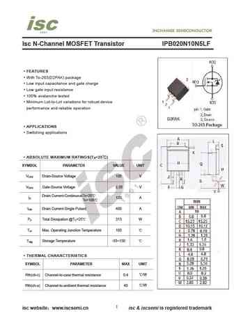
ipb020n10n5lf.pdf
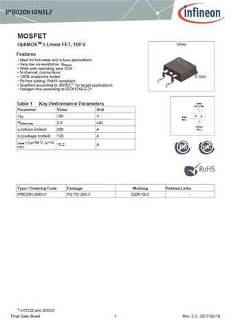
IPB020N10N5LF MOSFET D PAK OptiMOSTM 5 Linear FET, 100 V Features Ideal for hot-swap and e-fuse applications Very low on-resistance R DS(on) Wide safe operating area SOA N-channel, normal level 100% avalanche tested Pb-free plating; RoHS compliant Qualified according to JEDEC1) for target applications Halogen-free according to IEC61249-2-21 Drain ... See More ⇒
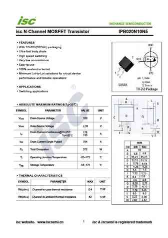
ipb020n10n5.pdf

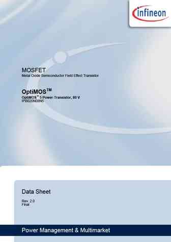
MOSFET Metal Oxide Semiconductor Field Effect Transistor OptiMOSTM OptiMOS 5 Power-Transistor, 100 V IPB020N10N5 Data Sheet Rev. 2.1 Final Power Management & Multimarket OptiMOS 5 Power-Transistor, 100 V IPB020N10N5 D PAK 1 Description Features N-channel, normal level Optimized for FOM OSS Very low on-resistance R DS(on) 175 C operating temperature ... See More ⇒
Detailed specifications: IPB011N04NG, IPB015N04LG, IPB015N04NG, IPB016N06L3G, IPB017N06N3G, IPB019N06L3G, IPB019N08N3G, IPB020N04NG, IRF540N, IPB021N06N3G, IPB022N04LG, IPB023N04NG, IPB023N06N3G, IPB025N08N3G, IPB025N10N3G, IPB027N10N3G, IPB029N06N3G
Keywords - IPB020NE7N3G MOSFET specs
IPB020NE7N3G cross reference
IPB020NE7N3G equivalent finder
IPB020NE7N3G pdf lookup
IPB020NE7N3G substitution
IPB020NE7N3G replacement
Need a MOSFET replacement? Our guide shows you how to find a perfect substitute by comparing key parameters and specs
🌐 : EN ES РУ

LIST
Last Update
MOSFET: AUP060N055 | AUP056N10 | AUP056N08BGL | AUP052N085 | AUP045N12 | AUP039N10 | AUP034N10 | AUP034N06 | AUP033N08BG | AUP026N085
Popular searches
2sc2078 | ac127 transistor | a42 transistor | bc547c | 2sa726 | 2sd313 | 2sc536 | d718 transistor