IPB042N10N3G Datasheet. Specs and Replacement
Type Designator: IPB042N10N3G 📄📄
Type of Transistor: MOSFET
Type of Control Channel: N-Channel
Absolute Maximum Ratings
Pd ⓘ - Maximum Power Dissipation: 214 W
|Vds|ⓘ - Maximum Drain-Source Voltage: 100 V
|Vgs|ⓘ - Maximum Gate-Source Voltage: 20 V
|Id| ⓘ - Maximum Drain Current: 100 A
Tj ⓘ - Maximum Junction Temperature: 175 °C
Electrical Characteristics
tr ⓘ - Rise Time: 59 nS
Cossⓘ - Output Capacitance: 1210 pF
RDSonⓘ - Maximum Drain-Source On-State Resistance: 0.0042 Ohm
Package: TO263
📄📄 Copy
IPB042N10N3G substitution
- MOSFET ⓘ Cross-Reference Search
IPB042N10N3G datasheet
..1. Size:976K infineon
ipb042n10n3g.pdf 
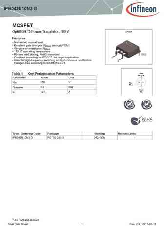
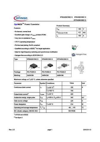
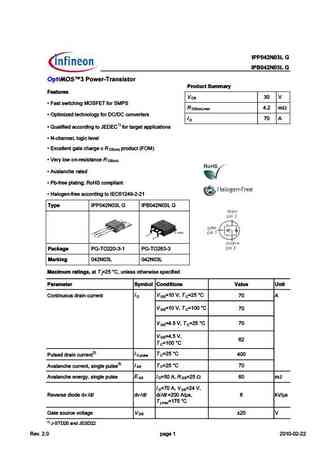
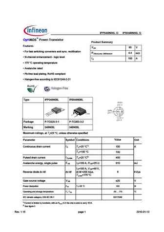
IPB042N10N3 G MOSFET D PAK OptiMOS 3 Power-Transistor, 100 V Features N-channel, normal level Excellent gate charge x R product (FOM) DS(on) Very low on-resistance R DS(on) 175 C operating temperature Pb-free lead plating; RoHS compliant Qualified according to JEDEC1) for target application Ideal for high-frequency switching and synchronous rectifica... See More ⇒
..2. Size:204K inchange semiconductor
ipb042n10n3g.pdf
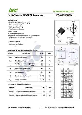
INCHANGE Semiconductor isc N-Channel MOSFET Transistor IPB042N10N3G FEATURES With TO-263(D2PAK) packaging Ultra-fast body diode High speed switching Very low on-resistence Easy to use 100% avalanche tested Minimum Lot-to-Lot variations for robust device performance and reliable operationz APPLICATIONS Switching applications ABSOLUTE MAXIMUM RATINGS(T =25 ) ... See More ⇒
7.1. Size:609K infineon
ipb042n03l.pdf
pe %% # ! % # ! F % (>.;?6?@ %>E Features D Q 2CD CG D49 ?8 ') - . 7@B -'*- 4 m - @? >2H Q ) AD > J65 D649?@=@8I 7@B 4@?F6BD6BC 7 D 1) Q + E2= 7 65 244@B5 ?8 D@ $ 7@B D2B86D 2AA= 42D @?C Q ( 492??6= =@8 4 =6F6= Q H46==6?D 82D6 492B86 H AB@5E4D ) ' D n) Q /6BI =@G @? B6C CD2?46 D n) Q F2=2?496 B2D65 Q *3 7B66 A=2D ?8 , @"- 4@>A= 2?D Q "2=@86... See More ⇒
9.1. Size:1005K 1
ipb048n15n5.pdf

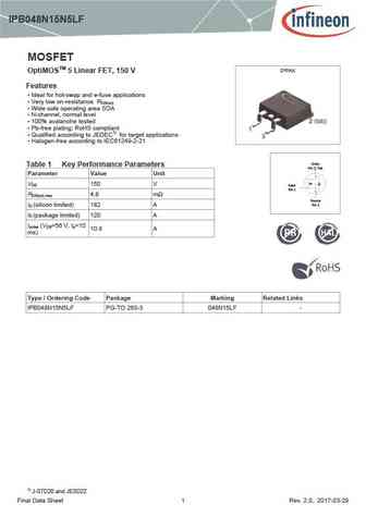
IPB048N15N5 MOSFET D PAK OptiMOS 5 Power-Transistor, 150 V Features tab Excellent gate charge x R product (FOM) DS(on) Very low on-resistance R DS(on) Very low reverse recovery charge (Qrr) 175 C operating temperature Pb-free lead plating; RoHS compliant Qualified according to JEDEC1) for target application 1 Ideal for high-frequency switching and ... See More ⇒
9.3. Size:871K infineon
ipb04cn10ng ipi04cn10n ipp04cn10n.pdf
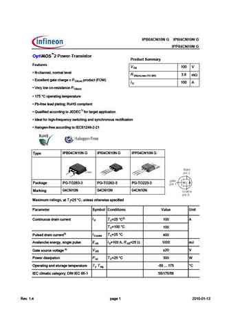
IPB04CN10N G IPI04CN10N G IPP04CN10N G 2 Power-Transistor Product Summary Features V 1 D R ( 492??6= ?@C>2= =6G6= R m - @? >2I .) R I46==6?E 82E6 492C86 I R AC@5F4E !) ' D n) I 1 D R /6CJ =@H @? C6D DE2?46 R D n) R U @A6C2E ?8 E6>A6C2EFC6 R *3 7C66 =625 A=2E ?8 , @#- 4@>A= 2?E 1) R + F2= 7 65 244@C5 ?8 E@ % 7@C E2C86E 2AA= 42E @? R $562= 7@C 9 89 7C6BF6?4J DH E4... See More ⇒
9.4. Size:683K infineon
ipb049n06l3g ipp052n06l3g ipp052n06l3 ipb049n06l3 ipp052n06l3 ipb052n06l3.pdf
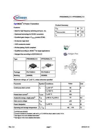
pe IPB049N06L3 G IPP052N06L3 G 3 Power-Transistor Product Summary Features V D R #562= 7@C 9 89 7C6BF6?4J DH E49 ?8 2?5 DJ?4 C64 R 4 7 m - @? >2I -' R ) AE > K65 E649?@=@8J 7@C 4@?G6CE6CD I D R I46==6?E 82E6 492C86 I R AC@5F4E ) ' D n) R ( 492??6= =@8 4 =6G6= R 2G2=2?496 E6DE65 R *3 7C66 A=2E ?8 , @"- 4@>A= 2?E 1) R + F2= 7 65 244@C5 ?8 E@ $ 7@C E2C86E 2AA= 42E ... See More ⇒
9.5. Size:899K infineon
ipb048n15n5lf.pdf
IPB048N15N5LF MOSFET D PAK OptiMOSTM 5 Linear FET, 150 V Features Ideal for hot-swap and e-fuse applications Very low on-resistance R DS(on) Wide safe operating area SOA N-channel, normal level 100% avalanche tested Pb-free plating; RoHS compliant Qualified according to JEDEC1) for target applications Halogen-free according to IEC61249-2-21 Drain ... See More ⇒
9.6. Size:347K infineon
ipb04n03la ipb04n03lat.pdf
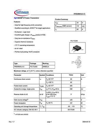
IPB04N03LA G OptiMOS 2 Power-Transistor Product Summary Features V 25 V DS Ideal for high-frequency dc/dc converters R (SMD version) 3.9 m DS(on),max Qualified according to JEDEC1) for target applications I 80 A D N-channel - Logic level Excellent gate charge x R product (FOM) DS(on) Very low on-resistance R DS(on) PG-TO263 Superior thermal resista... See More ⇒
9.7. Size:1130K infineon
ipb049n08n5.pdf
MOSFET Metal Oxide Semiconductor Field Effect Transistor OptiMOSTM OptiMOS 5 Power-Transistor, 80 V IPB049N08N5 Data Sheet Rev. 2.0 Final Power Management & Multimarket OptiMOS 5 Power-Transistor, 80 V IPB049N08N5 D PAK 1 Description Features Ideal for high frequency switching and sync. rec. Optimized technology for DC/DC converters Excellent gate charge x R pr... See More ⇒
9.9. Size:874K infineon
ipb04cn10ng ipi04cn10ng ipp04cn10ng ipp04cn10n .pdf

IPB04CN10N G IPI04CN10N G IPP04CN10N G 2 Power-Transistor Product Summary Features V 1 D R ( 492??6= ?@C>2= =6G6= R m - @? >2I .) R I46==6?E 82E6 492C86 I R AC@5F4E !) ' D n) I 1 D R /6CJ =@H @? C6D DE2?46 R D n) R U @A6C2E ?8 E6>A6C2EFC6 R *3 7C66 =625 A=2E ?8 , @#- 4@>A= 2?E 1) R + F2= 7 65 244@C5 ?8 E@ % 7@C E2C86E 2AA= 42E @? R $562= 7@C 9 89 7C6BF6?4J DH E4... See More ⇒
9.10. Size:1005K infineon
ipb048n15n5.pdf
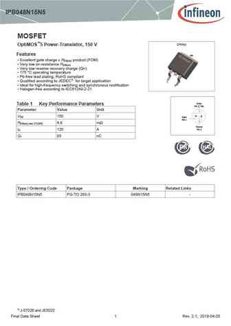
IPB048N15N5 MOSFET D PAK OptiMOS 5 Power-Transistor, 150 V Features tab Excellent gate charge x R product (FOM) DS(on) Very low on-resistance R DS(on) Very low reverse recovery charge (Qrr) 175 C operating temperature Pb-free lead plating; RoHS compliant Qualified according to JEDEC1) for target application 1 Ideal for high-frequency switching and ... See More ⇒
9.11. Size:734K infineon
ipb048n06lg ipp048n06lg5.pdf
IPP048N06L G IPB048N06L G Power-Transistor Product Summary Features V D P ?A 61BC BF9C389>7 3?>E5AC5AB 1>4 BH>3 A53C96931C9?> R 4 4 m , ?> =1G ,' E5AB9?> P ( 381>>581>35=5>C ... See More ⇒
9.12. Size:213K inchange semiconductor
ipb049ne7n3.pdf
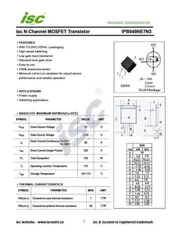
INCHANGE Semiconductor isc N-Channel MOSFET Transistor IPB049NE7N3 FEATURES With TO-263( D2PAK ) packaging High speed switching Low gate input resistance Standard level gate drive Easy to use 100% avalanche tested Minimum Lot-to-Lot variations for robust device performance and reliable operation APPLICATIONS Power supply Switching applications ABSOLUTE MAXI... See More ⇒
9.13. Size:229K inchange semiconductor
ipb048n15n5lf.pdf
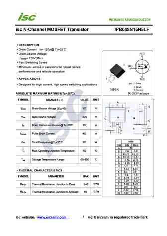
isc N-Channel MOSFET Transistor IPB048N15N5LF DESCRIPTION Drain Current I = 120A@ T =25 D C Drain Source Voltage V = 150V(Min) DSS Fast Switching Speed Minimum Lot-to-Lot variations for robust device performance and reliable operation APPLICATIONS . Designed for high current, high speed switching applications ABSOLUTE MAXIMUM RATINGS(T =25 ) C SYMBOL ARAMETER ... See More ⇒
9.14. Size:258K inchange semiconductor
ipb049n06l3.pdf
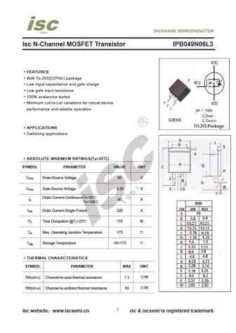
Isc N-Channel MOSFET Transistor IPB049N06L3 FEATURES With To-263(D2PAK) package Low input capacitance and gate charge Low gate input resistance 100% avalanche tested Minimum Lot-to-Lot variations for robust device performance and reliable operation APPLICATIONS Switching applications ABSOLUTE MAXIMUM RATINGS(T =25 ) a SYMBOL PARAMETER VALUE UNIT V Drain-Source V... See More ⇒
9.15. Size:205K inchange semiconductor
ipb049n08n5.pdf
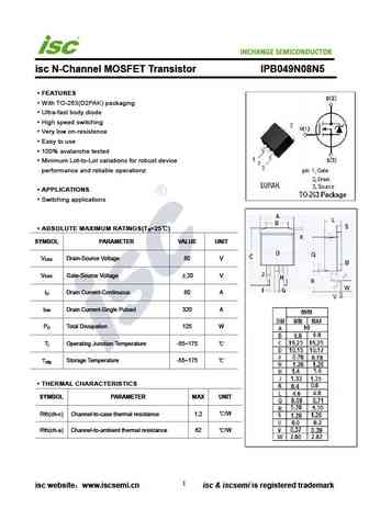
INCHANGE Semiconductor isc N-Channel MOSFET Transistor IPB049N08N5 FEATURES With TO-263(D2PAK) packaging Ultra-fast body diode High speed switching Very low on-resistence Easy to use 100% avalanche tested Minimum Lot-to-Lot variations for robust device performance and reliable operationz APPLICATIONS Switching applications ABSOLUTE MAXIMUM RATINGS(T =25 ) a... See More ⇒
9.16. Size:229K inchange semiconductor
ipb048n15n5.pdf
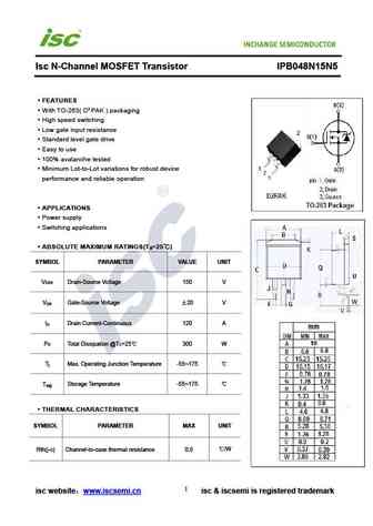
Isc N-Channel MOSFET Transistor IPB048N15N5 FEATURES With TO-263( D PAK ) packaging High speed switching Low gate input resistance Standard level gate drive Easy to use 100% avalanche tested Minimum Lot-to-Lot variations for robust device performance and reliable operation APPLICATIONS Power supply Switching applications ABSOLUTE MAXIMUM RATINGS(T =25 ) ... See More ⇒
9.17. Size:257K inchange semiconductor
ipb04cn10ng.pdf
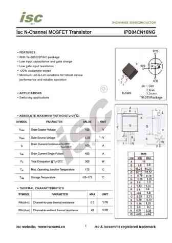
Isc N-Channel MOSFET Transistor IPB04CN10NG FEATURES With To-263(D2PAK) package Low input capacitance and gate charge Low gate input resistance 100% avalanche tested Minimum Lot-to-Lot variations for robust device performance and reliable operation APPLICATIONS Switching applications ABSOLUTE MAXIMUM RATINGS(T =25 ) a SYMBOL PARAMETER VALUE UNIT V Drain-Source V... See More ⇒
9.18. Size:258K inchange semiconductor
ipb041n04n.pdf
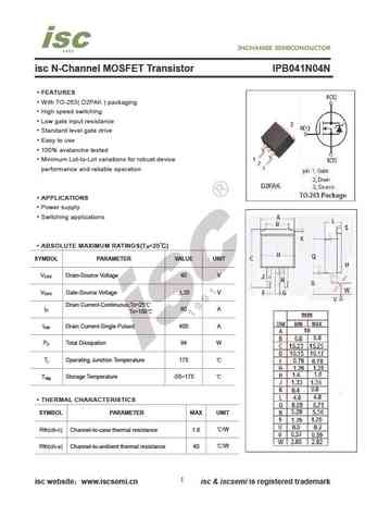
isc N-Channel MOSFET Transistor IPB041N04N FEATURES With TO-263( D2PAK ) packaging High speed switching Low gate input resistance Standard level gate drive Easy to use 100% avalanche tested Minimum Lot-to-Lot variations for robust device performance and reliable operation APPLICATIONS Power supply Switching applications ABSOLUTE MAXIMUM RATINGS(T =25 ) a ... See More ⇒
Detailed specifications: IPB035N08N3G, IPB036N12N3G, IPB037N06N3G, IPB038N12N3G, IPB039N04LG, IPB039N10N3G, IPB041N04NG, IPB042N03LG, IRFP250N, IPB048N06LG, IPB049N06L3G, IPB049NE7N3G, IPB050N06NG, IPB051NE8NG, IPB052N04NG, IPB054N06N3G, IPB054N08N3G
Keywords - IPB042N10N3G MOSFET specs
IPB042N10N3G cross reference
IPB042N10N3G equivalent finder
IPB042N10N3G pdf lookup
IPB042N10N3G substitution
IPB042N10N3G replacement
Step-by-step guide to finding a MOSFET replacement. Cross-reference parts and ensure compatibility for your repair or project.