IPD034N06N3G Specs and Replacement
Type Designator: IPD034N06N3G
Type of Transistor: MOSFET
Type of Control Channel: N-Channel
Absolute Maximum Ratings
Pd ⓘ
- Maximum Power Dissipation: 167 W
|Vds|ⓘ - Maximum Drain-Source Voltage: 60 V
|Vgs|ⓘ - Maximum Gate-Source Voltage: 20 V
|Id| ⓘ - Maximum Drain Current: 100 A
Tj ⓘ - Maximum Junction Temperature: 175 °C
Electrical Characteristics
tr ⓘ - Rise Time: 161 nS
Cossⓘ -
Output Capacitance: 1700 pF
RDSonⓘ - Maximum Drain-Source On-State Resistance: 0.0034 Ohm
Package: TO252
IPD034N06N3G substitution
- MOSFET ⓘ Cross-Reference Search
IPD034N06N3G datasheet
3.1. Size:436K infineon
ipd034n06n3.pdf 

pe # ! ! (TM) # A03 B53 4 m D n) m x Q ( @D9=9J54 D538>?F5BD5BC 1 D Q H35... See More ⇒
3.2. Size:243K inchange semiconductor
ipd034n06n3.pdf

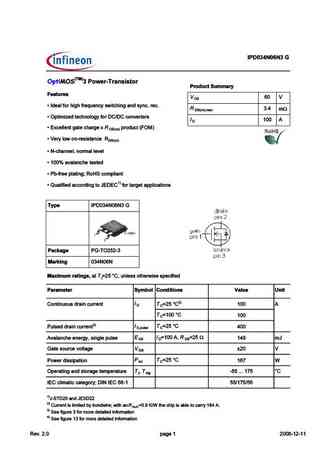
isc N-Channel MOSFET Transistor IPD034N06N3 IIPD034N06N3 FEATURES Static drain-source on-resistance RDS(on) 3.4m Enhancement mode 100% avalanche tested Minimum Lot-to-Lot variations for robust device performance and reliable operation DESCRITION High Frequency switching ABSOLUTE MAXIMUM RATINGS(T =25 ) a SYMBOL PARAMETER VALUE UNIT V Drain-Source Voltag... See More ⇒
9.1. Size:423K infineon
ipd038n04n.pdf
pe $ " " $;B1= '=- >5>?;= $=;0@/? &@99-=D Features 4 D P 1BC BF9C389>7 &( , - 6?A ,&), m D n) m x P ( @C9=9I54 C538>?E5AC5AB D 1) P * D17 C? $ 6?A C1A75C 1@@B P ' 381>>5?A=1... See More ⇒
9.2. Size:400K infineon
ipd03n03lag.pdf
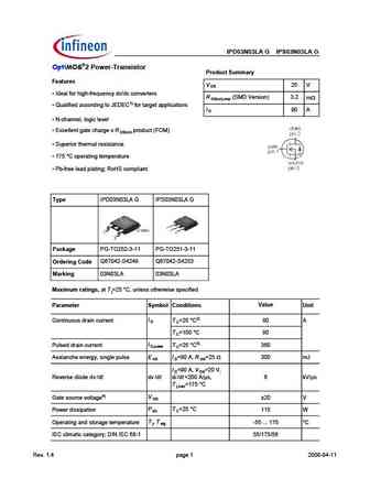
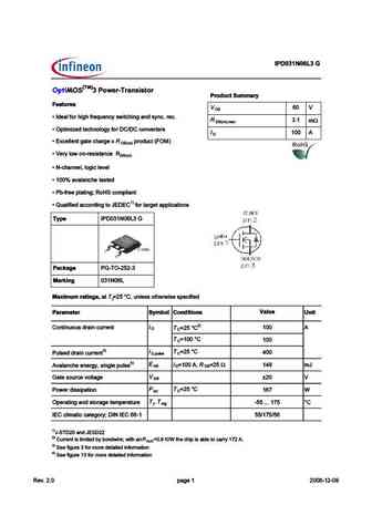
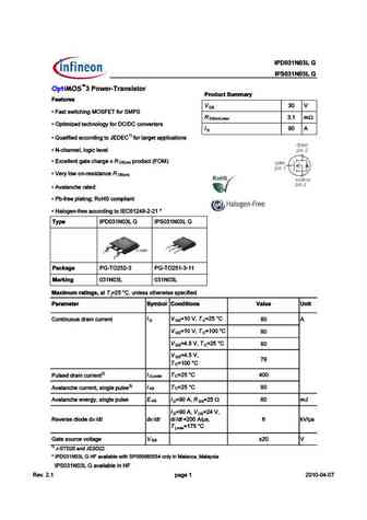
IPD03N03LA G IPS03N03LA G OptiMOS 2 Power-Transistor Product Summary Features V 25 V DS Ideal for high-frequency dc/dc converters R (SMD Version) 3.2 m DS(on),max Qualified according to JEDEC1) for target applications I 90 A D N-channel, logic level Excellent gate charge x R product (FOM) DS(on) Superior thermal resistance 175 C operating temperatu... See More ⇒
9.3. Size:668K infineon
ipd031n03l.pdf

pe % # ! %' # ! % (>.;?6?@ %>E Features V D R !3DE DH;E5 ;@9 (* .! / 8AC .(+. R 1 m D n) m x R * BE;?;K76 E75 @A>A9J 8AC 5A@G7CE7CD I D 1) R , F3>;8;76 355AC6;@9 EA % 8AC E3C97E 3BB>;53E;A@D R ) 5 3@@7> >A9;5 >7G7> R I57>>7@E 93E7 5 3C97 I R BCA6F5E !* ( D n) R 07CJ >AH A@ C7D;DE3@57 R D n) R G3>3@5 7 C3E76 R +4 8C77 B>3E;@9 - A#. 5A?B>;3@E R #... See More ⇒
9.5. Size:429K infineon
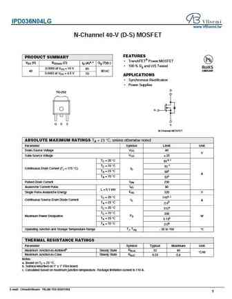
ipd036n04l.pdf
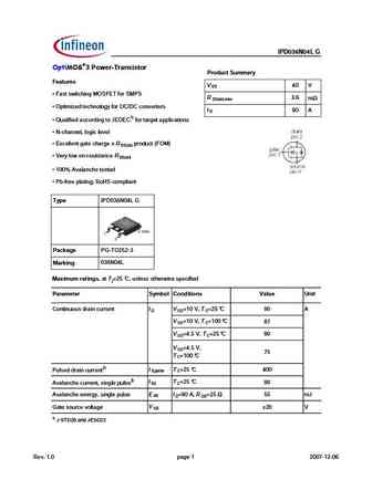
pe % # ! % (>.;?6?@ %>E Features V 4 D Q 2CD CG D49 ?8 ') - . 7@B -'*- R m D n) m x Q ) AD > J65 D649?@=@8I 7@B 4@?F6BD6BC I D 1) Q + E2= 7 65 244@B5 ?8 D@ $ 7@B D2B86D 2AA= 42D @?C Q ( 492??6= =@8 4 =6F6= Q H46==6?D 82D6 492B86 H R AB@5E4D ) ' D n) Q /6BI =@G @? B6C CD2?46 R D n) Q F2=2?496 D6CD65 Q *3 7B66 A=2D ?8 , @"- 4@>A= 2?D Type #* ( ... See More ⇒
9.6. Size:153K infineon
ipd036n04lg.pdf
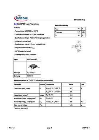
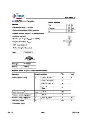
Type IPD036N04L G OptiMOS 3 Power-Transistor Product Summary Features V 40 V DS Fast switching MOSFET for SMPS R 3.6 m DS(on),max Optimized technology for DC/DC converters I 90 A D Qualified according to JEDEC1) for target applications N-channel, logic level Excellent gate charge x R product (FOM) DS(on) Very low on-resistance R DS(on) 100% Av... See More ⇒
9.7. Size:445K infineon
ipd031n06l3.pdf
pe % # ! % (>.;?6?@ %>E Features D R #562= 7@C 9 89 7C6BF6?4J DH E49 ?8 2?5 DJ?4 C64 1 m D n) m x R ) AE > K65 E649?@=@8J 7@C 4@?G6CE6CD 1 D R I46==6?E 82E6 492C86 I AC@5F4E ) ' D n) R /6CJ =@H @? C6D DE2?46 , D n) R ( 492??6= =@8 4 =6G6= R 2G2=2?496 E6DE65 R *3 7C66 A=2E ?8 , @"- 4@>A= 2?E 1) R + F2= 7 65 244@C5 ?8 E@ $ 7@C E2C86E 2AA= 42E @?D Ty... See More ⇒
9.8. Size:865K infineon
ipd033n06n.pdf
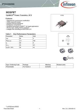
IPD033N06N MOSFET D-PAK OptiMOSTM Power-Transistor, 60 V Features Optimized for synchronous rectification tab 100% avalanche tested Superior thermal resistance N-channel, normal level 1 2 Qualified according to JEDEC1) for target applications Pb-free lead plating; RoHS compliant 3 Halogen-free according to IEC61249-2-21 Table 1 Key Performance Paramete... See More ⇒
9.9. Size:444K infineon
ipd035n06l3.pdf

pe % # ! % (>.;?6?@ %>E Features D R #562= 7@C 9 89 7C6BF6?4J DH E49 ?8 2?5 DJ?4 C64 m D n) m x R ) AE > K65 E649?@=@8J 7@C 4@?G6CE6CD D R I46==6?E 82E6 492C86 I AC@5F4E ) ' D n) R /6CJ =@H @? C6D DE2?46 , D n) R ( 492??6= =@8 4 =6G6= R 2G2=2?496 E6DE65 R *3 7C66 A=2E ?8 , @"- 4@>A= 2?E 1) R + F2= 7 65 244@C5 ?8 E@ $ 7@C E2C86E 2AA= 42E @?D Type #* (... See More ⇒
9.10. Size:671K infineon
ipd031n03lg ips031n03lg.pdf
pe % # ! %' # ! % (>.;?6?@ %>E Features V D R !3DE DH;E5 ;@9 (* .! / 8AC .(+. R 1 m D n) m x R * BE;?;K76 E75 @A>A9J 8AC 5A@G7CE7CD I D 1) R , F3>;8;76 355AC6;@9 EA % 8AC E3C97E 3BB>;53E;A@D R ) 5 3@@7> >A9;5 >7G7> R I57>>7@E 93E7 5 3C97 I R BCA6F5E !* ( D n) R 07CJ >AH A@ C7D;DE3@57 R D n) R G3>3@5 7 C3E76 R +4 8C77 B>3E;@9 - A#. 5A?B>;3@E R #... See More ⇒
9.11. Size:2552K cn vbsemi
ipd036n04lg.pdf
IPD036N04LG www.VBsemi.tw N-Channel 40-V (D-S) MOSFET FEATURES PRODUCT SUMMARY TrenchFET Power MOSFET VDS (V) RDS(on) ( ) ID (A)a, c Qg (Typ.) 100 % Rg and UIS Tested RoHS 0.0050 at VGS = 10 V 85 COMPLIANT 40 80 nC 0.0065 at VGS = 4.5 V 70 APPLICATIONS Synchronous Rectification Power Supplies D TO-252 G G D S S N-Channel MOSFET ABSOLUTE MAXIMUM ... See More ⇒
9.12. Size:243K inchange semiconductor
ipd038n06n3.pdf
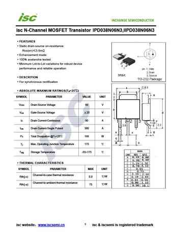
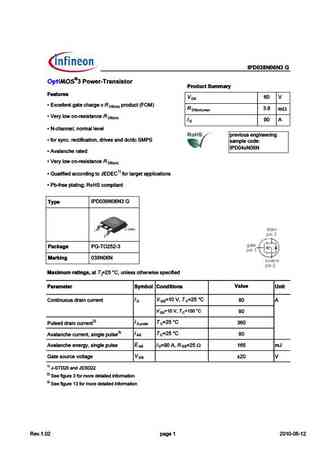
isc N-Channel MOSFET Transistor IPD038N06N3,IIPD038N06N3 FEATURES Static drain-source on-resistance RDS(on) 3.8m Enhancement mode 100% avalanche tested Minimum Lot-to-Lot variations for robust device performance and reliable operation DESCRITION For synchronous rectification ABSOLUTE MAXIMUM RATINGS(T =25 ) a SYMBOL PARAMETER VALUE UNIT V Drain-Source Volta... See More ⇒
9.13. Size:241K inchange semiconductor
ipd031n03l.pdf

isc N-Channel MOSFET Transistor IPD031N03L, IIPD031N03L FEATURES Static drain-source on-resistance RDS(on) 3.1m Enhancement mode 100% avalanche tested Minimum Lot-to-Lot variations for robust device performance and reliable operation DESCRITION Fast switching ABSOLUTE MAXIMUM RATINGS(T =25 ) a SYMBOL PARAMETER VALUE UNIT V Drain-Source Voltage 30 V DSS V ... See More ⇒
9.14. Size:242K inchange semiconductor
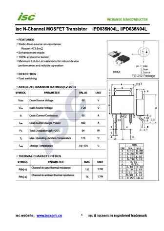
ipd036n04l.pdf
isc N-Channel MOSFET Transistor IPD036N04L, IIPD036N04L FEATURES Static drain-source on-resistance RDS(on) 3.6m Enhancement mode 100% avalanche tested Minimum Lot-to-Lot variations for robust device performance and reliable operation DESCRITION Fast switching ABSOLUTE MAXIMUM RATINGS(T =25 ) a SYMBOL PARAMETER VALUE UNIT V Drain-Source Voltage 60 V DSS V ... See More ⇒
9.15. Size:242K inchange semiconductor
ipd031n06l3.pdf
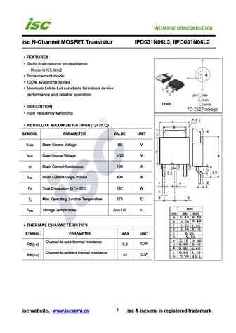
isc N-Channel MOSFET Transistor IPD031N06L3, IIPD031N06L3 FEATURES Static drain-source on-resistance RDS(on) 3.1m Enhancement mode 100% avalanche tested Minimum Lot-to-Lot variations for robust device performance and reliable operation DESCRITION High frequency switching ABSOLUTE MAXIMUM RATINGS(T =25 ) a SYMBOL PARAMETER VALUE UNIT V Drain-Source Voltage 6... See More ⇒
9.16. Size:242K inchange semiconductor
ipd033n06n.pdf

isc N-Channel MOSFET Transistor IPD033N06N, IIPD033N06N FEATURES Static drain-source on-resistance RDS(on) 3.3m Enhancement mode 100% avalanche tested Minimum Lot-to-Lot variations for robust device performance and reliable operation DESCRITION Optimized for synchronous rectification ABSOLUTE MAXIMUM RATINGS(T =25 ) a SYMBOL PARAMETER VALUE UNIT V Drain-Sou... See More ⇒
Detailed specifications: IPD90N06S4-07, IPD90N06S4L-03, IPD90N06S4L-05, IPD90N06S4L-06, IPD90P03P4-04, IPD90P03P4L-04, IPD031N03LG, IPD031N06L3G, 2N60, IPD035N06L3G, IPD036N04LG, IPD038N04NG, IPD038N06N3G, IPD040N03LG, IPD042P03L3G, IPD048N06L3G, IPD050N03LG
Keywords - IPD034N06N3G MOSFET specs
IPD034N06N3G cross reference
IPD034N06N3G equivalent finder
IPD034N06N3G pdf lookup
IPD034N06N3G substitution
IPD034N06N3G replacement
Can't find your MOSFET?
Learn how to find a substitute transistor by analyzing voltage, current and package compatibility