SPD02N80C3 Specs and Replacement
Type Designator: SPD02N80C3
Type of Transistor: MOSFET
Type of Control Channel: N-Channel
Absolute Maximum Ratings
Pd ⓘ - Maximum Power Dissipation: 42 W
|Vds|ⓘ - Maximum Drain-Source Voltage: 800 V
|Vgs|ⓘ - Maximum Gate-Source Voltage: 20 V
|Id| ⓘ - Maximum Drain Current: 2 A
Tj ⓘ - Maximum Junction Temperature: 150 °C
Electrical Characteristics
tr ⓘ - Rise Time: 15 nS
Cossⓘ - Output Capacitance: 13 pF
Rds ⓘ - Maximum Drain-Source On-State Resistance: 2.7 Ohm
Package: TO252
SPD02N80C3 substitution
- MOSFET ⓘ Cross-Reference Search
SPD02N80C3 datasheet
spd02n80c3.pdf
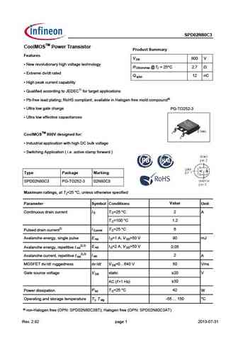
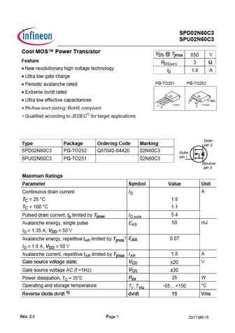
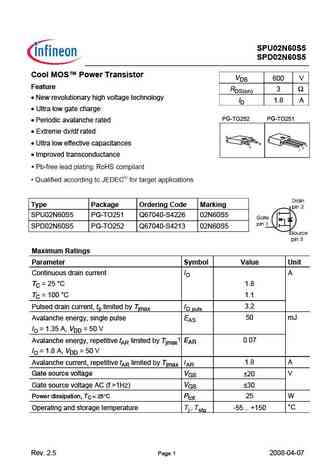
SPD02N80C3 CoolMOSTM Power Transistor Product Summary Features V 800 V DS New revolutionary high voltage technology R @ Tj = 25 C 2.7 W DS(on)max Extreme dv/dt rated Q 12 nC g,typ High peak current capability Qualified according to JEDEC1) for target applications Pb-free lead plating; RoHS compliant; available in Halogen free mold compounda) Ultra low ga... See More ⇒
spd02n80c3.pdf
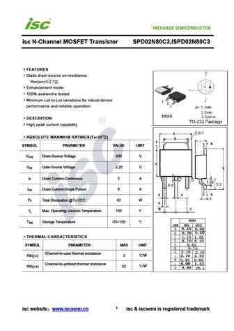
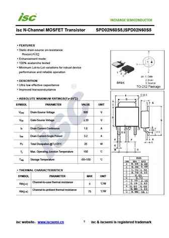
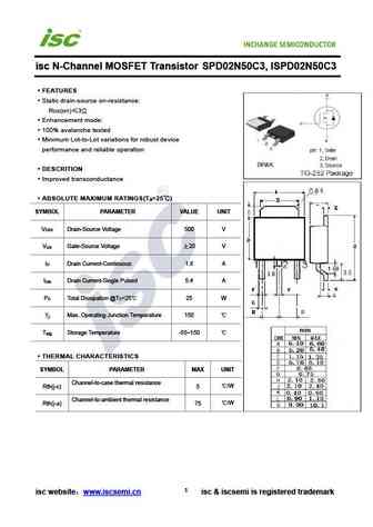
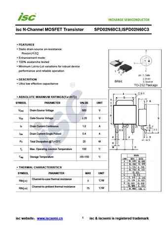
isc N-Channel MOSFET Transistor SPD02N80C3,ISPD02N80C3 FEATURES Static drain-source on-resistance RDS(on) 2.7 Enhancement mode 100% avalanche tested Minimum Lot-to-Lot variations for robust device performance and reliable operation DESCRITION High peak current capability ABSOLUTE MAXIMUM RATINGS(T =25 ) a SYMBOL PARAMETER VALUE UNIT V Drain-Source Voltage 8... See More ⇒
spd02n60.pdf
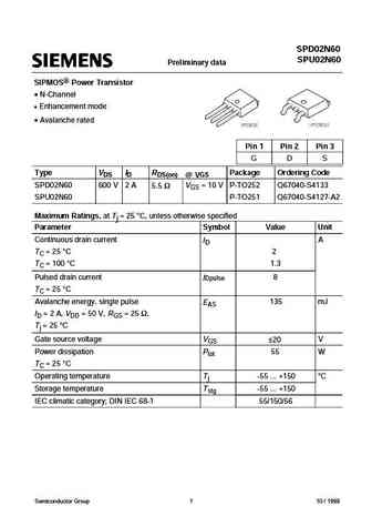
SPD02N60 SPU02N60 Preliminary data SIPMOS Power Transistor N-Channel Enhancement mode Avalanche rated Pin 1 Pin 2 Pin 3 G D S Type VDS ID RDS(on) @ VGS Package Ordering Code SPD02N60 600 V 2 A VGS = 10 V P-TO252 Q67040-S4133 5.5 SPU02N60 P-TO251 Q67040-S4127-A2 Maximum Ratings, at Tj = 25 C, unless otherwise specified Parameter Symbol Value Unit Continuous d... See More ⇒
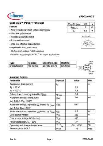

Detailed specifications: SPB20N60S5 , SPB21N50C3 , SPB80N10LG , SPB80P06PG , SPD01N60C3 , SPD02N50C3 , SPD02N60C3 , SPD02N60S5 , STP65NF06 , SPD03N50C3 , SPD03N60C3 , SPD03N60S5 , SPD04N50C3 , SPD04N60C3 , SPD04N60S5 , SPD04N80C3 , SPD04P10PG .
Keywords - SPD02N80C3 MOSFET specs
SPD02N80C3 cross reference
SPD02N80C3 equivalent finder
SPD02N80C3 pdf lookup
SPD02N80C3 substitution
SPD02N80C3 replacement
Learn how to find the right MOSFET substitute. A guide to cross-reference, check specs and replace MOSFETs in your circuits.


LIST
Last Update
MOSFET: AOI780A70 | AOB42S60L | AOTF950A70L | AOTF27S60L | AOTF11S60L | AONV070V65G1 | AOM065V120X2Q | AOM033V120X2 | AOK500V120X2 | AOK065V65X2
Popular searches
2sc2580 | 2sc710 | 2sc968 | 2sd217 | bdw93c equivalent | cs7n60f | d613 transistor | fdmc8884 mosfet