SSM6J06FU Specs and Replacement
Type Designator: SSM6J06FU
Type of Transistor: MOSFET
Type of Control Channel: P-Channel
Absolute Maximum Ratings
Pd ⓘ
- Maximum Power Dissipation: 0.3 W
|Vds|ⓘ - Maximum Drain-Source Voltage: 20 V
|Vgs|ⓘ - Maximum Gate-Source Voltage: 12 V
|Id| ⓘ - Maximum Drain Current: 0.65 A
Tj ⓘ - Maximum Junction Temperature: 150 °C
Electrical Characteristics
Cossⓘ -
Output Capacitance: 90 pF
RDSonⓘ - Maximum Drain-Source On-State Resistance: 0.5 Ohm
Package: SOT363
SC88
US6
- MOSFET ⓘ Cross-Reference Search
SSM6J06FU datasheet
..1. Size:189K toshiba
ssm6j06fu.pdf 
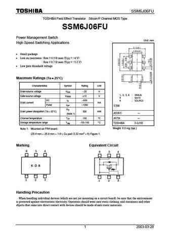
SSM6J06FU TOSHIBA Field Effect Transistor Silicon P Channel MOS Type SSM6J06FU Power Management Switch Unit mm High Speed Switching Applications Small package Low on resistance Ron = 0.5 max (V = -4 V) GS Ron = 0.7 max (V = -2.5 V) GS Low gate threshold voltage Maximum Ratings (Ta = = 25 C) = = Characteristics Symbol Rating Unit Drain-sourc... See More ⇒
8.1. Size:136K toshiba
ssm6j07fu.pdf
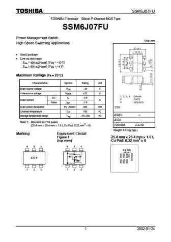
SSM6J07FU TOSHIBA Transistor Silicon P Channel MOS Type SSM6J07FU Power Management Switch Unit mm High Speed Switching Applications Small package Low on resistance R = 450 m (max) (V = -10 V) on GS Ron = 800 m (max) (VGS = -4 V) Maximum Ratings (Ta = = 25 C) = = Characteristics Symbol Rating Unit Drain-source voltage VDS -30 V Gate-source voltage V... See More ⇒
8.2. Size:152K toshiba
ssm6j08fu.pdf
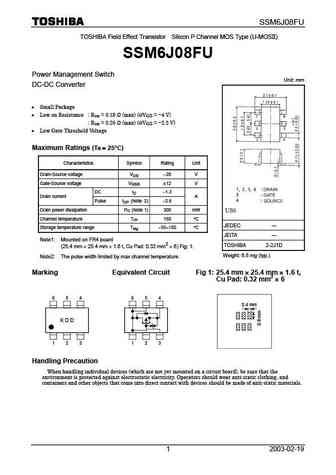
SSM6J08FU TOSHIBA Field Effect Transistor Silicon P Channel MOS Type (U-MOSII) SSM6J08FU Power Management Switch Unit mm DC-DC Converter Small Package Low on Resistance R = 0.18 (max) (@V = -4 V) on GS R = 0.26 (max) (@V = -2.5 V) on GS Low Gate Threshold Voltage Maximum Ratings (Ta = = 25 C) = = Characteristics Symbol Rating Unit Drain-Sour... See More ⇒
9.1. Size:222K toshiba
ssm6j771g.pdf
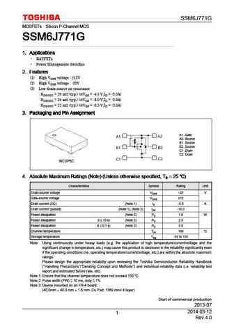
SSM6J771G MOSFETs Silicon P-Channel MOS SSM6J771G SSM6J771G SSM6J771G SSM6J771G 1. Applications 1. Applications 1. Applications 1. Applications BATFETs Power Management Switches 2. Features 2. Features 2. Features 2. Features (1) High VGSS voltage 12V (2) High VDSS voltage -20V (3) Low drain-source on-resistance RDS(ON) = 26 m (typ.) (@VGS = -4.5 V,ID = -3.... See More ⇒
9.2. Size:240K toshiba
ssm6j507nu.pdf
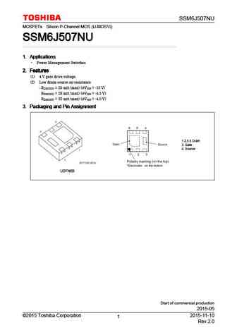
SSM6J507NU MOSFETs Silicon P-Channel MOS (U-MOS ) SSM6J507NU SSM6J507NU SSM6J507NU SSM6J507NU 1. Applications 1. Applications 1. Applications 1. Applications Power Management Switches 2. Features 2. Features 2. Features 2. Features (1) 4 V gate drive voltage. (2) Low drain-source on-resistance RDS(ON) = 20 m (max) (@VGS = -10 V) RDS(ON) = 28 m (max) (@VGS = -4.5... See More ⇒
9.3. Size:277K toshiba
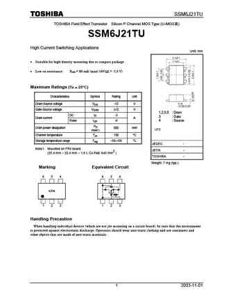
ssm6j51tu.pdf
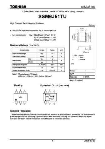
SSM6J51TU TOSHIBA Field Effect Transistor Silicon P Channel MOS Type (U-MOS ) SSM6J51TU High Current Switching Applications Unit mm Suitable for high-density mounting due to compact package Low on-resistance Ron = 54 m (max) (@VGS = -2.5 V) 85 m (max) (@VGS = -1.8 V) 150m (max) (@VGS = -1.5 V) Maximum Ratings (Ta = 25 C) Characteristics Symbol Rating Unit... See More ⇒
9.4. Size:197K toshiba
ssm6j402tu.pdf
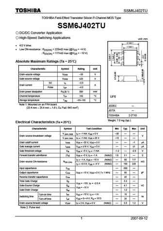
SSM6J402TU TOSHIBA Field-Effect Transistor Silicon P-Channel MOS Type SSM6J402TU DC/DC Converter Application High-Speed Switching Applications unit mm 2.1 0.1 4.0 V drive 1.7 0.1 Low ON-resistance RDS(ON) = 225m max (@VGS = -4 V) RDS(ON) = 117m max (@VGS = -10 V) 1 6 2 5 Absolute Maximum Ratings (Ta = 25 C) 3 4 Characteristic Symbol Rating ... See More ⇒
9.5. Size:305K toshiba
ssm6j206fe.pdf
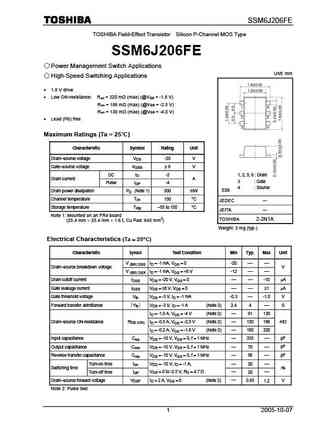
SSM6J206FE TOSHIBA Field-Effect Transistor Silicon P-Channel MOS Type SSM6J206FE Power Management Switch Applications Unit mm High-Speed Switching Applications 1.8 V drive Low ON-resistance Ron = 320 m (max) (@VGS = -1.8 V) Ron = 186 m (max) (@VGS = -2.5 V) R = 130 m (max) (@V = -4.0 V) on GS Lead (Pb) free Maximum Ratings (Ta = 25 C) Cha... See More ⇒
9.6. Size:152K toshiba
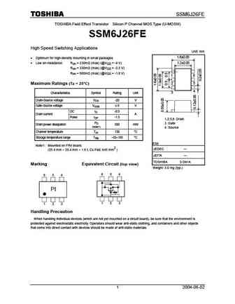
ssm6j25fe.pdf
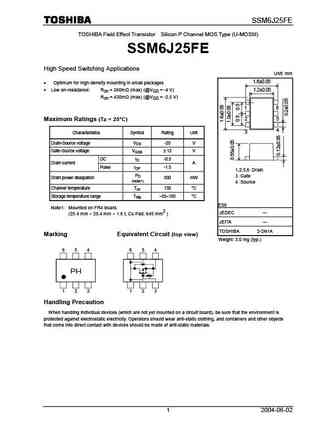
SSM6J25FE TOSHIBA Field Effect Transistor Silicon P Channel MOS Type (U-MOSIII) SSM6J25FE High Speed Switching Applications Unit mm 1.6 0.05 Optimum for high-density mounting in small packages Low on-resistance Ron = 260m (max) (@VGS = -4 V) 1.2 0.05 Ron = 430m (max) (@VGS = -2.5 V) 1 6 5 Maximum Ratings (Ta = 25 C) 2 4 3 Characteristics Symbol Rating Uni... See More ⇒
9.7. Size:217K toshiba
ssm6j410tu.pdf
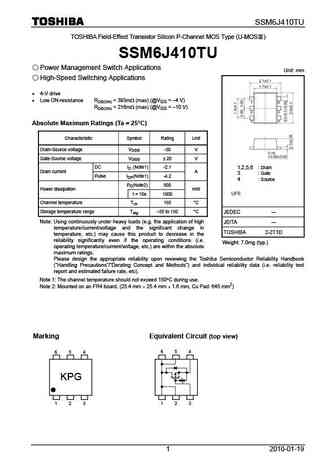
SSM6J410TU TOSHIBA Field-Effect Transistor Silicon P-Channel MOS Type (U-MOS ) SSM6J410TU Power Management Switch Applications Unit mm High-Speed Switching Applications 4-V drive Low ON-resistance RDS(ON) = 393m (max) (@VGS = 4 V) RDS(ON) = 216m (max) (@VGS = 10 V) Absolute Maximum Ratings (Ta = 25 C) Characteristic Symbol Rating Unit Drain-Sou... See More ⇒
9.8. Size:221K toshiba
ssm6j409tu.pdf
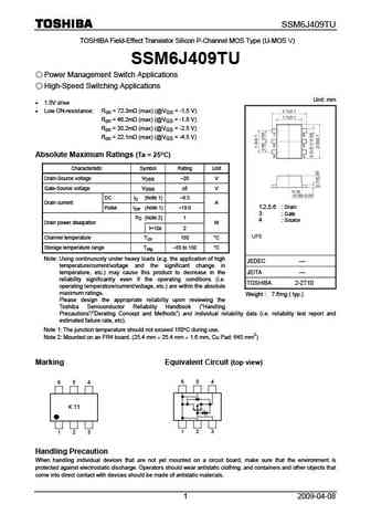
SSM6J409TU TOSHIBA Field-Effect Transistor Silicon P-Channel MOS Type (U-MOS V) SSM6J409TU Power Management Switch Applications High-Speed Switching Applications Unit mm 1.5V drive Low ON-resistance Ron = 72.3m (max) (@VGS = -1.5 V) Ron = 46.2m (max) (@VGS = -1.8 V) Ron = 30.2m (max) (@VGS = -2.5 V) Ron = 22.1m (max) (@VGS = -4.5 V) Absolut... See More ⇒
9.9. Size:370K toshiba
ssm6j512nu.pdf
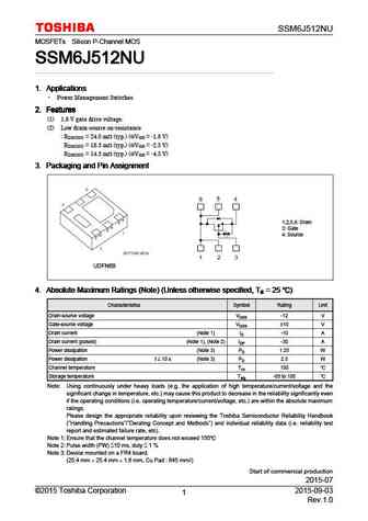
SSM6J512NU MOSFETs Silicon P-Channel MOS SSM6J512NU SSM6J512NU SSM6J512NU SSM6J512NU 1. Applications 1. Applications 1. Applications 1. Applications Power Management Switches 2. Features 2. Features 2. Features 2. Features (1) 1.8 V gate drive voltage. (2) Low drain-source on-resistance RDS(ON) = 24.0 m (typ.) (@VGS = -1.8 V) RDS(ON) = 18.3 m (typ.) (@VGS = -2.5 V... See More ⇒
9.10. Size:295K toshiba
ssm6j511nu.pdf
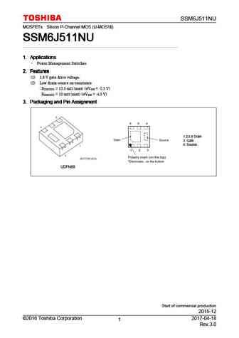
SSM6J511NU MOSFETs Silicon P-Channel MOS (U-MOS ) SSM6J511NU SSM6J511NU SSM6J511NU SSM6J511NU 1. Applications 1. Applications 1. Applications 1. Applications Power Management Switches 2. Features 2. Features 2. Features 2. Features (1) 1.8 V gate drive voltage. (2) Low drain-source on-resistance RDS(ON) = 13.5 m (max) (@VGS = -2.5 V) RDS(ON) = 10 m (max) (@VGS =... See More ⇒
9.11. Size:250K toshiba
ssm6j23fe.pdf
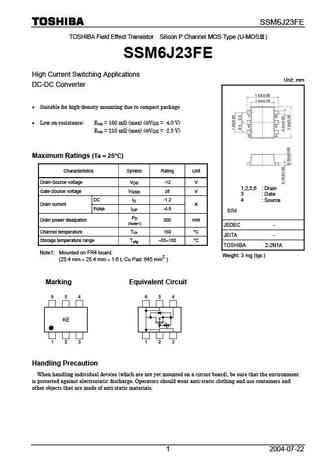
SSM6J23FE TOSHIBA Field Effect Transistor Silicon P Channel MOS Type (U-MOS ) SSM6J23FE High Current Switching Applications Unit mm DC-DC Converter Suitable for high-density mounting due to compact package Low on-resistance Ron = 160 m (max) (@VGS = -4.0 V) Ron = 210 m (max) (@VGS = -2.5 V) Maximum Ratings (Ta = 25 C) Characteristics Symbol Rating Unit Dra... See More ⇒
9.12. Size:299K toshiba
ssm6j53fe.pdf
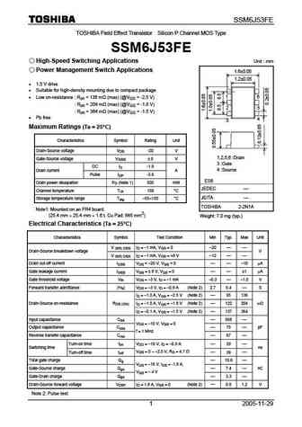
SSM6J53FE TOSHIBA Field Effect Transistor Silicon P Channel MOS Type SSM6J53FE High-Speed Switching Applications Unit mm Power Management Switch Applications 1.6 0.05 1.2 0.05 1.5 V drive Suitable for high-density mounting due to compact package 1 6 Low on-resistance Ron = 136 m (max) (@VGS = -2.5 V) Ron = 204 m (max) (@VGS = -1.8 V) 5 2 ... See More ⇒
9.13. Size:202K toshiba
ssm6j213fe.pdf
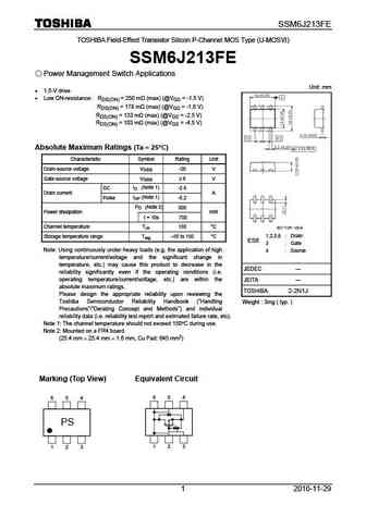
SSM6J213FE TOSHIBA Field-Effect Transistor Silicon P-Channel MOS Type (U-MOS ) SSM6J213FE Power Management Switch Applications Unit mm 1.5-V drive Low ON-resistance RDS(ON) = 250 m (max) (@VGS = -1.5 V) RDS(ON) = 178 m (max) (@VGS = -1.8 V) RDS(ON) = 133 m (max) (@VGS = -2.5 V) RDS(ON) = 103 m (max) (@VGS = -4.5 V) Absolute Maximum Ratings (Ta = 25... See More ⇒
9.14. Size:237K toshiba
ssm6j503nu.pdf
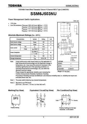
SSM6J503NU TOSHIBA Field-Effect Transistor Silicon P-Channel MOS Type (U-MOS ) SSM6J503NU Power Management Switch Applications Unit mm 1.5V drive Low ON-resistance RDS(ON)= 89.6 m (max) (@VGS = -1.5 V) RDS(ON) = 57.9 m (max) (@VGS = -1.8 V) RDS(ON) = 41.7 m (max) (@VGS = -2.5 V) RDS(ON) = 32.4 m (max) (@VGS = -4.5 V) Absolute Maximum Ratings (Ta = 25 C... See More ⇒
9.15. Size:218K toshiba
ssm6j205fe.pdf
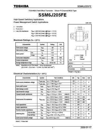
SSM6J205FE TOSHIBA Field-Effect Transistor Silicon P-Channel MOS Type SSM6J205FE High-Speed Switching Applications Power Management Switch Applications Unit mm 1.8V drive P-ch 2-in-1 Low ON-resistance Ron = 460 m (max) (@VGS = -1.8 V) Ron = 306 m (max) (@VGS = -2.5 V) Ron = 234 m (max) (@VGS = -4.0 V) Maximum Ratings (Ta = 25 C) Characteristic Sym... See More ⇒
9.16. Size:205K toshiba
ssm6j412tu.pdf
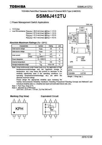
SSM6J412TU TOSHIBA Field-Effect Transistor Silicon P-Channel MOS Type (U-MOS ) SSM6J412TU Power Management Switch Applications Unit mm 2.1 0.1 1.5-V drive 1.7 0.1 Low ON-resistance RDS(ON) = 99.6 m (max) (@VGS = -1.5 V) RDS(ON) = 67.8 m (max) (@VGS = -1.8 V) RDS(ON) = 51.4 m (max) (@VGS = -2.5 V) 1 6 RDS(ON) = 42.7 m (max) (@VGS = -4.5 V) 5 2 A... See More ⇒
9.17. Size:226K toshiba
ssm6j215fe.pdf
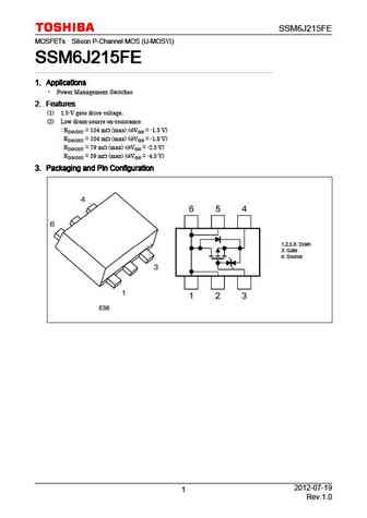
SSM6J215FE MOSFETs Silicon P-Channel MOS (U-MOS ) SSM6J215FE SSM6J215FE SSM6J215FE SSM6J215FE 1. Applications 1. Applications 1. Applications 1. Applications Power Management Switches 2. Features 2. Features 2. Features 2. Features (1) 1.5-V gate drive voltage. (2) Low drain-source on-resistance RDS(ON) = 154 m (max) (@VGS = -1.5 V) RDS(ON) = 104 m (max) (@VGS =... See More ⇒
9.18. Size:157K toshiba
ssm6j21tu.pdf
SSM6J21TU TOSHIBA Field Effect Transistor Silicon P Channel MOS Type (U-MOS ) SSM6J21TU High Current Switching Applications Unit mm Suitable for high-density mounting due to compact package Low on resistance Ron = 88 m (max) (@VGS = -2.5 V) Maximum Ratings (Ta = 25 C) Characteristics Symbol Rating Unit Drain-Source voltage VDS -12 V Gate-Source voltage VGSS 12... See More ⇒
9.19. Size:215K toshiba
ssm6j216fe.pdf
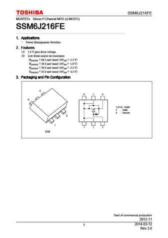
SSM6J216FE MOSFETs Silicon P-Channel MOS (U-MOS ) SSM6J216FE SSM6J216FE SSM6J216FE SSM6J216FE 1. Applications 1. Applications 1. Applications 1. Applications Power Management Switches 2. Features 2. Features 2. Features 2. Features (1) 1.5-V gate drive voltage. (2) Low drain-source on-resistance RDS(ON) = 88.1 m (max) (@VGS = -1.5 V) RDS(ON) = 56.0 m (max) (@VGS... See More ⇒
9.20. Size:236K toshiba
ssm6j502nu.pdf
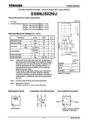
SSM6J502NU TOSHIBA Field Effect Transistor Silicon P Channel MOS Type(U-MOS ) SSM6J502NU Power Management Switch Applications Unit mm 1.5V drive Low ON-resistance RDS(ON) = 60.5 m (max) (@VGS = -1.5 V) RDS(ON) = 38.4 m (max) (@VGS = -1.8 V) RDS(ON) = 28.3 m (max) (@VGS = -2.5 V) RDS(ON) = 23.1 m (max) (@VGS = -4.5 V) Absolute Maximum Ratings (Ta = 25 C... See More ⇒
9.21. Size:241K toshiba
ssm6j50tu.pdf
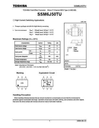
SSM6J50TU TOSHIBA Field Effect Transistor Silicon P Channel MOS Type (U-MOS ) SSM6J50TU High Current Switching Applications Unit mm Compact package suitable for high-density mounting Low on-resistance Ron = 205m (max) (@VGS = -2.0 V) Ron = 100m (max) (@VGS = -2.5 V) Ron = 64m (max) (@VGS = -4.5 V) Maximum Ratings (Ta = 25 C) Characteristics Symbol Ra... See More ⇒
9.22. Size:205K toshiba
ssm6j501nu.pdf
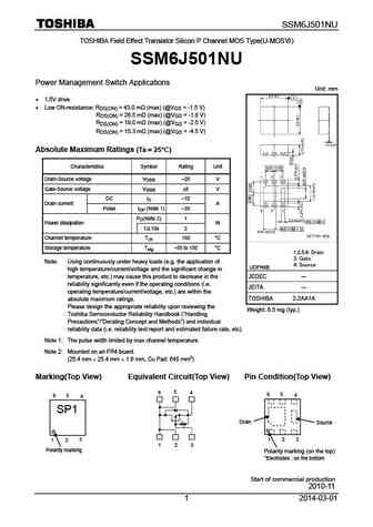
SSM6J501NU TOSHIBA Field Effect Transistor Silicon P Channel MOS Type(U-MOS ) SSM6J501NU Power Management Switch Applications Unit mm 1.5V drive Low ON-resistance RDS(ON) = 43.0 m (max) (@VGS = -1.5 V) RDS(ON) = 26.5 m (max) (@VGS = -1.8 V) RDS(ON) = 19.0 m (max) (@VGS = -2.5 V) RDS(ON) = 15.3 m (max) (@VGS = -4.5 V) Absolute Maximum Ratings (Ta = 25 C... See More ⇒
9.23. Size:235K toshiba
ssm6j505nu.pdf
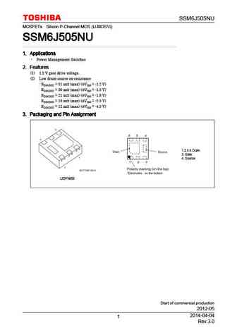
SSM6J505NU MOSFETs Silicon P-Channel MOS (U-MOS ) SSM6J505NU SSM6J505NU SSM6J505NU SSM6J505NU 1. Applications 1. Applications 1. Applications 1. Applications Power Management Switches 2. Features 2. Features 2. Features 2. Features (1) 1.2 V gate drive voltage. (2) Low drain-source on-resistance RDS(ON) = 61 m (max) (@VGS = -1.2 V) RDS(ON) = 30 m (max) (@VGS = -... See More ⇒
9.24. Size:154K toshiba
ssm6j26fe.pdf
SSM6J26FE TOSHIBA Field Effect Transistor Silicon P Channel MOS Type (U-MOSIII) SSM6J26FE High Speed Switching Applications Unit mm 1.6 0.05 Optimum for high-density mounting in small packages Low on-resistance Ron = 230m (max) (@VGS = -4 V) 1.2 0.05 Ron = 330m (max) (@VGS = -2.5 V) Ron = 980m (max) (@VGS = -1.8 V) 1 6 5 Maximum Ratings (Ta = 25 C) 2 4... See More ⇒
9.25. Size:207K toshiba
ssm6j214fe.pdf
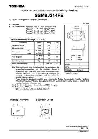
SSM6J214FE TOSHIBA Field-Effect Transistor Silicon P-Channel MOS Type (U-MOS ) SSM6J214FE Power Management Switch Applications Unit mm 1.8 V drive Low ON-resistance RDS(ON) = 149.6 m (max) (@VGS = -1.8 V) RDS(ON) = 77.6 m (max) (@VGS = -2.5 V) RDS(ON) = 57.0 m (max) (@VGS = -4.5 V) RDS(ON) = 50.0 m (max) (@VGS = -10 V) Absolute Maximum Ratings (Ta... See More ⇒
9.26. Size:190K toshiba
ssm6j212fe.pdf
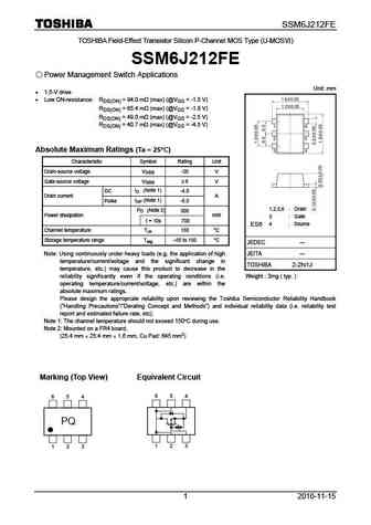
SSM6J212FE TOSHIBA Field-Effect Transistor Silicon P-Channel MOS Type (U-MOS ) SSM6J212FE Power Management Switch Applications Unit mm 1.5-V drive Low ON-resistance RDS(ON) = 94.0 m (max) (@VGS = -1.5 V) RDS(ON) = 65.4 m (max) (@VGS = -1.8 V) RDS(ON) = 49.0 m (max) (@VGS = -2.5 V) RDS(ON) = 40.7 m (max) (@VGS = -4.5 V) Absolute Maximum Ratings (Ta ... See More ⇒
9.27. Size:215K toshiba
ssm6j414tu.pdf
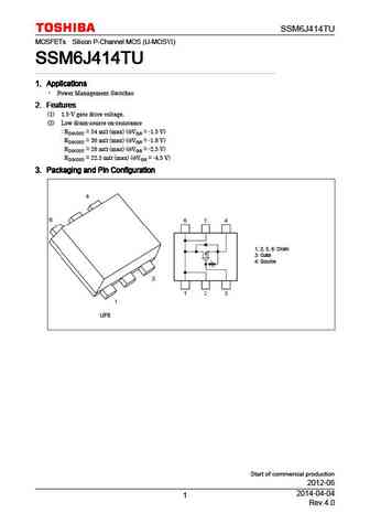
SSM6J414TU MOSFETs Silicon P-Channel MOS (U-MOS ) SSM6J414TU SSM6J414TU SSM6J414TU SSM6J414TU 1. Applications 1. Applications 1. Applications 1. Applications Power Management Switches 2. Features 2. Features 2. Features 2. Features (1) 1.5-V gate drive voltage. (2) Low drain-source on-resistance RDS(ON) = 54 m (max) (@VGS = -1.5 V) RDS(ON) = 36 m (max) (@VGS = -... See More ⇒
9.28. Size:312K toshiba
ssm6j207fe.pdf
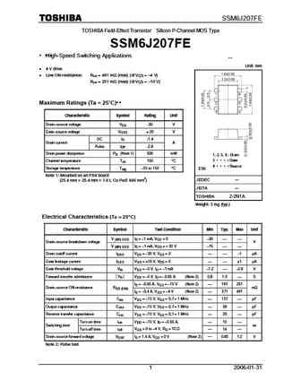
SSM6J207FE TOSHIBA Field-Effect Transistor Silicon P-Channel MOS Type SSM6J207FE High-Speed Switching Applications Unit mm 4 V drive Low ON-resistance Ron = 491 m (max) (@VGS = -4 V) Ron = 251 m (max) (@VGS = -10 V) Maximum Ratings (Ta = 25 C) Characteristic Symbol Rating Unit Drain source voltage VDS -30 V Gate source voltage VGSS 20 V DC ID -1.4... See More ⇒
9.29. Size:197K toshiba
ssm6j401tu.pdf
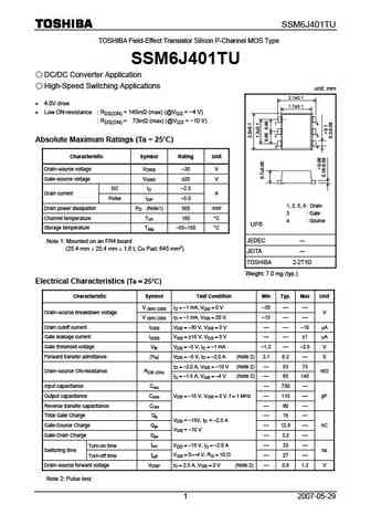
SSM6J401TU TOSHIBA Field-Effect Transistor Silicon P-Channel MOS Type SSM6J401TU DC/DC Converter Application High-Speed Switching Applications unit mm 2.1 0.1 4.0V drive 1.7 0.1 Low ON-resistance RDS(ON) = 145m (max) (@VGS = -4 V) RDS(ON) = 73m (max) (@VGS = -10 V) 1 6 2 5 Absolute Maximum Ratings (Ta = 25 C) 3 4 Characteristic Symbol Rating... See More ⇒
Detailed specifications: SSM5N15FE, SSM5N15FU, SSM5N16FE, SSM5N16FU, SSM5P05FU, SSM5P15FU, SSM5P16FE, SSM5P16FU, AON7506, SSM6J07FU, SSM6J08FU, SSM6J205FE, SSM6J206FE, SSM6J207FE, SSM6J212FE, SSM6J213FE, SSM6J214FE
Keywords - SSM6J06FU MOSFET specs
SSM6J06FU cross reference
SSM6J06FU equivalent finder
SSM6J06FU pdf lookup
SSM6J06FU substitution
SSM6J06FU replacement
Need a MOSFET replacement?
Our guide shows you how to find a perfect substitute by comparing key parameters and specs
