TK13A65D Specs and Replacement
Type Designator: TK13A65D
Type of Transistor: MOSFET
Type of Control Channel: N-Channel
Absolute Maximum Ratings
Pd ⓘ - Maximum Power Dissipation: 50 W
|Vds|ⓘ - Maximum Drain-Source Voltage: 650 V
|Vgs|ⓘ - Maximum Gate-Source Voltage: 30 V
|Id| ⓘ - Maximum Drain Current: 13 A
Tj ⓘ - Maximum Junction Temperature: 150 °C
Electrical Characteristics
tr ⓘ - Rise Time: 50 nS
Cossⓘ - Output Capacitance: 280 pF
RDSonⓘ - Maximum Drain-Source On-State Resistance: 0.47 Ohm
Package: TO220SIS
TK13A65D substitution
- MOSFET ⓘ Cross-Reference Search
TK13A65D datasheet
tk13a65d.pdf
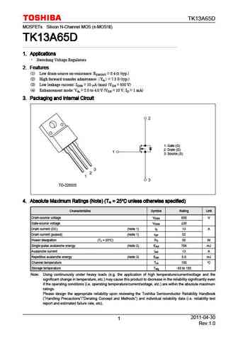
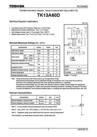
TK13A65D MOSFETs Silicon N-Channel MOS ( -MOS ) TK13A65D TK13A65D TK13A65D TK13A65D 1. Applications 1. Applications 1. Applications 1. Applications Switching Voltage Regulators 2. Features 2. Features 2. Features 2. Features (1) Low drain-source on-resistance RDS(ON) = 0.4 (typ.) (2) High forward transfer admittance Yfs = 7.5 S (typ.) (3) Low leakage current IDS... See More ⇒
tk13a65d.pdf
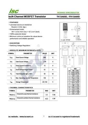
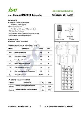
INCHANGE Semiconductor iscN-Channel MOSFET Transistor TK13A65D ITK13A65D FEATURES Low drain-source on-resistance RDS(on) = 0.4 (typ.) Enhancement mode Vth = 2.0 to 4.0V (VDS = 10 V, ID=1.0mA) 100% avalanche tested Minimum Lot-to-Lot variations for robust device performance and reliable operation DESCRITION Switching Voltage Regulators ABSOLUTE MAXIMUM RATINGS(... See More ⇒
tk13a65u.pdf
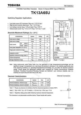
TK13A65U TOSHIBA Field Effect Transistor Silicon N Channel MOS Type (DTMOS II) TK13A65U Switching Regulator Applications Unit mm 2.7 0.2 10 0.3 3.2 0.2 A Low drain-source ON resistance RDS (ON) = 0.32 (typ.) High forward transfer admittance Yfs = 8.0 S (typ.) Low leakage current IDSS = 100 A (max) (VDS = 650 V) Enhancement-mod... See More ⇒
tk13a65u.pdf
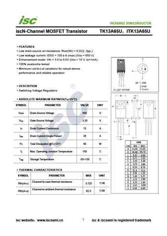
INCHANGE Semiconductor iscN-Channel MOSFET Transistor TK13A65U ITK13A65U FEATURES Low drain-source on-resistance RDS(ON) = 0.32 (typ.) Low leakage current IDSS = 100 A (max) (VDS = 650 V) Enhancement mode Vth = 3.0 to 5.0V (VDS = 10 V, ID=1mA) 100% avalanche tested Minimum Lot-to-Lot variations for robust device performance and reliable operation DESCRITION Sw... See More ⇒
Detailed specifications: TK12X60U, TK130F06K3, TK13A25D, TK13A45D, TK13A50DA, TK13A50D, TK13A55DA, TK13A60D, IRF640, TK13A65U, TK13E25D, TK13J65U, TK13P25D, TK14A45DA, TK14A45D, TK14A55D, TK150F04K3
Keywords - TK13A65D MOSFET specs
TK13A65D cross reference
TK13A65D equivalent finder
TK13A65D pdf lookup
TK13A65D substitution
TK13A65D replacement
Can't find your MOSFET? Learn how to find a substitute transistor by analyzing voltage, current and package compatibility
History: SSPL6005 | AP4533GEH-HF
🌐 : EN ES РУ

LIST
Last Update
MOSFET: AKF30N5P0SX | AKF30N10S | AKF20P45D | CM4407 | CM3407 | CM3400 | SVF11N65F | SVF11N65T | FKBB3105 | EHBA036R1
Popular searches
2sc1913 | c2314 transistor | c2482 transistor | 2sc1222 replacement | 2sa725 | c5242 transistor | 2sa726 replacement | a1941 datasheet