BUK552-100A Specs and Replacement
Type Designator: BUK552-100A
Type of Transistor: MOSFET
Type of Control Channel: N-Channel
Absolute Maximum Ratings
Pd ⓘ
- Maximum Power Dissipation: 60 W
|Vds|ⓘ - Maximum Drain-Source Voltage: 100 V
|Id| ⓘ - Maximum Drain Current: 5.5 A
Tj ⓘ - Maximum Junction Temperature: 150 °C
Electrical Characteristics
RDSonⓘ - Maximum Drain-Source On-State Resistance: 0.28 Ohm
Package: SOT78
- MOSFET ⓘ Cross-Reference Search
BUK552-100A datasheet
0.1. Size:56K philips
buk552-100a-b 1.pdf 

Philips Semiconductors Product Specification PowerMOS transistor BUK552-100A/B Logic level FET GENERAL DESCRIPTION QUICK REFERENCE DATA N-channel enhancement mode SYMBOL PARAMETER MAX. MAX. UNIT logic level field-effect power transistor in a plastic envelope. BUK552 -100A -100B The device is intended for use in VDS Drain-source voltage 100 100 V Switched Mode Power Supplies ID Drain ... See More ⇒
7.1. Size:55K philips
buk552-60a-b 1.pdf

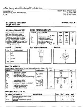
Philips Semiconductors Product Specification PowerMOS transistor BUK552-60A/B Logic level FET GENERAL DESCRIPTION QUICK REFERENCE DATA N-channel enhancement mode SYMBOL PARAMETER MAX. MAX. UNIT logic level field-effect power transistor in a plastic envelope. BUK552 -60A -60B The device is intended for use in VDS Drain-source voltage 60 60 V Switched Mode Power Supplies ID Drain curre... See More ⇒
9.1. Size:55K philips
buk555-200a-b 1.pdf

Philips Semiconductors Product Specification PowerMOS transistor BUK555-200A/B Logic level FET GENERAL DESCRIPTION QUICK REFERENCE DATA N-channel enhancement mode SYMBOL PARAMETER MAX. MAX. UNIT logic level field-effect power transistor in a plastic envelope. BUK555 -200A -200B The device is intended for use in VDS Drain-source voltage 200 200 V Switched Mode Power Supplies ID Drain ... See More ⇒
9.2. Size:53K philips
buk556-60h 1.pdf
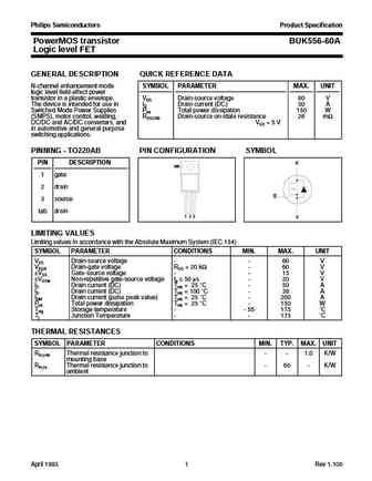
Philips Semiconductors Product Specification PowerMOS transistor BUK556-60H Logic level FET GENERAL DESCRIPTION QUICK REFERENCE DATA N-channel enhancement mode logic SYMBOL PARAMETER MAX. UNIT level field-effect power transistor in a plastic envelope. VDS Drain-source voltage 60 V The device is intended for use in ID Drain current (DC) 60 A automotive and general purpose Ptot Total p... See More ⇒
9.3. Size:60K philips
buk553-100b.pdf

Philips Semiconductors Product Specification PowerMOS transistor BUK553-100A/B Logic level FET GENERAL DESCRIPTION QUICK REFERENCE DATA N-channel enhancement mode SYMBOL PARAMETER MAX. MAX. UNIT logic level field-effect power transistor in a plastic envelope. BUK553 -100A -100B The device is intended for use in VDS Drain-source voltage 100 100 V Switched Mode Power Supplies ID Drain ... See More ⇒
9.4. Size:55K philips
buk555-60a-b 1.pdf

Philips Semiconductors Product Specification PowerMOS transistor BUK555-60A/B Logic level FET GENERAL DESCRIPTION QUICK REFERENCE DATA N-channel enhancement mode SYMBOL PARAMETER MAX. MAX. UNIT logic level field-effect power transistor in a plastic envelope. BUK555 -60A -60B The device is intended for use in VDS Drain-source voltage 60 60 V Switched Mode Power Supplies ID Drain curre... See More ⇒
9.5. Size:69K philips
buk553-48c 1.pdf
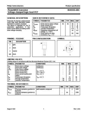
Philips Semiconductors Product specification PowerMOS transistor BUK553-48C Voltage clamped logic level FET GENERAL DESCRIPTION QUICK REFERENCE DATA Protected N-channel enhancement SYMBOL PARAMETER MIN. TYP. MAX. UNIT mode logic level field-effect power transistor in a plastic envelope. V(CL)DSR Drain-source clamp voltage 40 48 58 V The device is intended for use in ID Drain current (... See More ⇒
9.6. Size:54K philips
buk553-60a-b 1.pdf

Philips Semiconductors Product Specification PowerMOS transistor BUK553-60A/B Logic level FET GENERAL DESCRIPTION QUICK REFERENCE DATA N-channel enhancement mode SYMBOL PARAMETER MAX. MAX. UNIT logic level field-effect power transistor in a plastic envelope. BUK553 -60A -60B The device is intended for use in VDS Drain-source voltage 60 60 V Switched Mode Power Supplies ID Drain curre... See More ⇒
9.7. Size:56K philips
buk553-100a-b 1.pdf
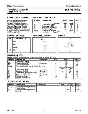
Philips Semiconductors Product Specification PowerMOS transistor BUK553-100A/B Logic level FET GENERAL DESCRIPTION QUICK REFERENCE DATA N-channel enhancement mode SYMBOL PARAMETER MAX. MAX. UNIT logic level field-effect power transistor in a plastic envelope. BUK553 -100A -100B The device is intended for use in VDS Drain-source voltage 100 100 V Switched Mode Power Supplies ID Drain ... See More ⇒
9.8. Size:69K philips
buk555-60h 1.pdf
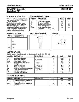
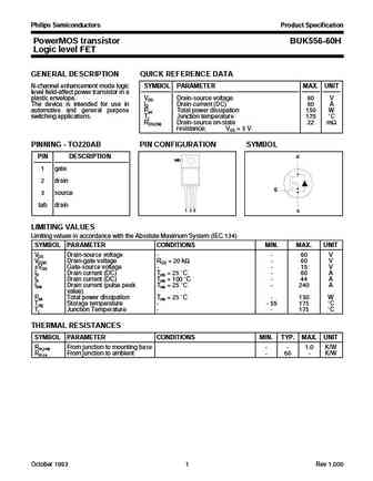
Philips Semiconductors Product specification PowerMOS transistor BUK555-60H Logic level FET GENERAL DESCRIPTION QUICK REFERENCE DATA N-channel enhancement mode logic SYMBOL PARAMETER MAX. UNIT level field-effect power transistor in a plastic envelope. VDS Drain-source voltage 60 V The device is intended for use in ID Drain current (DC) 41 A Automotive applications, Switched Ptot Tota... See More ⇒
9.9. Size:63K philips
buk554-60h 1.pdf
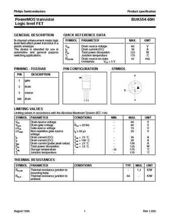
Philips Semiconductors Product specification PowerMOS transistor BUK554-60H Logic level FET GENERAL DESCRIPTION QUICK REFERENCE DATA N-channel enhancement mode logic SYMBOL PARAMETER MAX. UNIT level field-effect power transistor in a plastic envelope VDS Drain-source voltage 60 V The device is intended for use in ID Drain current (DC) 39 A automotive and general purpose Ptot Total po... See More ⇒
9.10. Size:54K philips
buk555-100a-b 1.pdf

Philips Semiconductors Product Specification PowerMOS transistor BUK555-100A/B Logic level FET GENERAL DESCRIPTION QUICK REFERENCE DATA N-channel enhancement mode SYMBOL PARAMETER MAX. MAX. UNIT logic level field-effect power transistor in a plastic envelope. BUK555 -100A -100B The device is intended for use in VDS Drain-source voltage 100 100 V Switched Mode Power Supplies ID Drain ... See More ⇒
9.11. Size:86K philips
buk555-200b.pdf
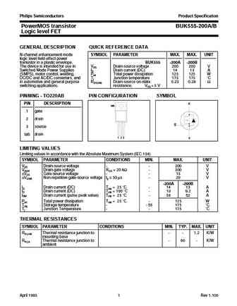
Philips Semiconductors Product Specification PowerMOS transistor BUK555-200A/B Logic level FET GENERAL DESCRIPTION QUICK REFERENCE DATA N-channel enhancement mode SYMBOL PARAMETER MAX. MAX. UNIT logic level field-effect power transistor in a plastic envelope. BUK555 -200A -200B The device is intended for use in VDS Drain-source voltage 200 200 V Switched Mode Power Supplies ID Drain ... See More ⇒
9.12. Size:53K philips
buk556-60a 1.pdf
Philips Semiconductors Product Specification PowerMOS transistor BUK556-60A Logic level FET GENERAL DESCRIPTION QUICK REFERENCE DATA N-channel enhancement mode SYMBOL PARAMETER MAX. UNIT logic level field-effect power transistor in a plastic envelope. VDS Drain-source voltage 60 V The device is intended for use in ID Drain current (DC) 50 A Switched Mode Power Supplies Ptot Total pow... See More ⇒
9.14. Size:234K inchange semiconductor
buk555-100.pdf
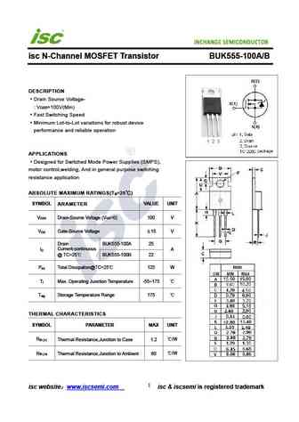
INCHANGE Semiconductor isc N-Channel MOSFET Transistor BUK555-100A/B DESCRIPTION Drain Source Voltage- V =100V(Min) DSS Fast Switching Speed Minimum Lot-to-Lot variations for robust device performance and reliable operation APPLICATIONS Designed for Switched Mode Power Supplies (SMPS), motor control,welding, And in general purpose switching resistance application ABSOLUTE... See More ⇒
Detailed specifications: BUK465-200A
, BUK466-200A
, BUK473-100A
, BUK473-100B
, BUK482-100A
, BUK543-100A
, BUK545-100A
, BUK545-100B
, 2N7002
, BUK552-100B
, BUK553-100A
, BUK555-100A
, BUK555-100B
, BUK555-200A
, BUK563-100A
, BUK565-100A
, BUK581-100A
.
History: BUK553-100A
Keywords - BUK552-100A MOSFET specs
BUK552-100A cross reference
BUK552-100A equivalent finder
BUK552-100A pdf lookup
BUK552-100A substitution
BUK552-100A replacement
Learn how to find the right MOSFET substitute. A guide to cross-reference, check specs and replace MOSFETs in your circuits.