2SK3567 Datasheet. Specs and Replacement
Type Designator: 2SK3567 📄📄
Type of Transistor: MOSFET
Type of Control Channel: N-Channel
Absolute Maximum Ratings
Pd ⓘ - Maximum Power Dissipation: 35 W
|Vds|ⓘ - Maximum Drain-Source Voltage: 600 V
|Vgs|ⓘ - Maximum Gate-Source Voltage: 30 V
|Id| ⓘ - Maximum Drain Current: 3.5 A
Tj ⓘ - Maximum Junction Temperature: 150 °C
Electrical Characteristics
tr ⓘ - Rise Time: 12 nS
Cossⓘ - Output Capacitance: 60 pF
RDSonⓘ - Maximum Drain-Source On-State Resistance: 2.2 Ohm
Package: TO220SIS
📄📄 Copy
- MOSFET ⓘ Cross-Reference Search
2SK3567 datasheet
..1. Size:223K toshiba
2sk3567.pdf 
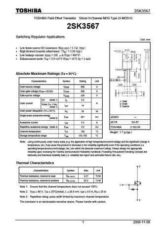
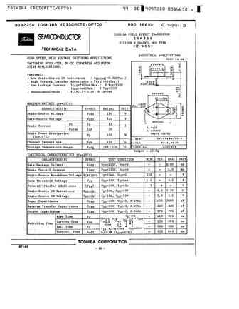
2SK3567 TOSHIBA Field Effect Transistor Silicon N Channel MOS Type ( -MOSVI) 2SK3567 Switching Regulator Applications Unit mm Low drain-source ON resistance RDS (ON) = 1.7 (typ.) High forward transfer admittance Yfs = 2.5S (typ.) Low leakage current IDSS = 100 A (VDS = 600 V) Enhancement mode Vth = 2.0 4.0 V (VDS = 10 V, ID = 1 mA) Absolute Maximum ... See More ⇒
..2. Size:280K inchange semiconductor
2sk3567.pdf

isc N-Channel MOSFET Transistor 2SK3567 FEATURES Drain Current I = 3.5A@ T =25 D C Drain Source Voltage V = 600V(Min) DSS Static Drain-Source On-Resistance R = 2.2 (Max) @ V = 10V DS(on) GS 100% avalanche tested Minimum Lot-to-Lot variations for robust device performance and reliable operation DESCRIPTION motor drive, DC-DC converter, power switch and soleno... See More ⇒
8.1. Size:214K toshiba
2sk3566.pdf
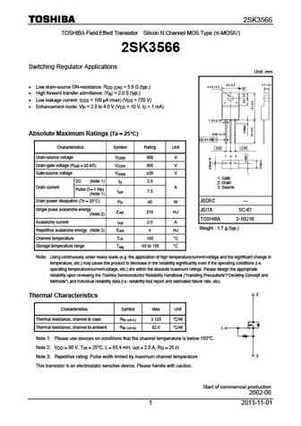
2SK3566 TOSHIBA Field Effect Transistor Silicon N Channel MOS Type ( -MOSIV) 2SK3566 Switching Regulator Applications Unit mm Low drain-source ON-resistance RDS (ON) = 5.6 (typ.) High forward transfer admittance Yfs = 2.0 S (typ.) Low leakage current IDSS = 100 A (max) (VDS = 720 V) Enhancement mode Vth = 2.0 to 4.0 V (VDS = 10 V, ID = 1 mA) Absol... See More ⇒
8.2. Size:227K toshiba
2sk3565.pdf

2SK3565 TOSHIBA Field Effect Transistor Silicon N Channel MOS Type ( -MOSIV) 2SK3565 Switching Regulator Applications Unit mm Low drain-source ON resistance RDS (ON) = 2.0 (typ.) High forward transfer admittance Yfs = 4.5 S (typ.) Low leakage current IDSS = 100 A (VDS = 720 V) Enhancement mode Vth = 2.0 to 4.0 V (VDS = 10 V, ID = 1 mA) Absolute Ma... See More ⇒
8.3. Size:233K toshiba
2sk3569.pdf
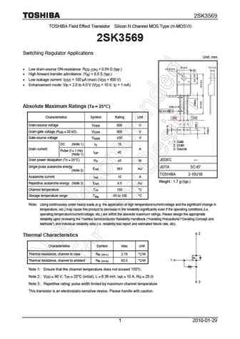
2SK3569 TOSHIBA Field Effect Transistor Silicon N Channel MOS Type ( -MOSVI) 2SK3569 Switching Regulator Applications Unit mm Low drain-source ON-resistance RDS (ON) = 0.54 (typ.) High forward transfer admittance Yfs = 8.5 S (typ.) Low leakage current IDSS = 100 A (max) (VDS = 600 V) Enhancement mode Vth = 2.0 to 4.0 V (VDS = 10 V, ID = 1 mA) Abso... See More ⇒
8.4. Size:227K toshiba
2sk3561.pdf
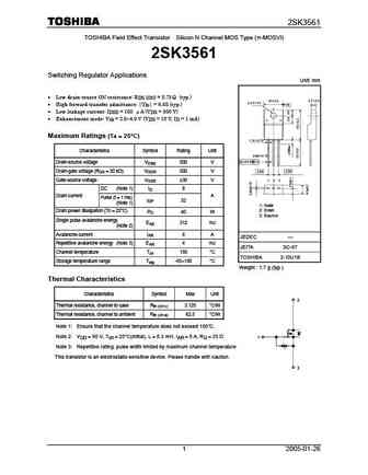
2SK3561 TOSHIBA Field Effect Transistor Silicon N Channel MOS Type ( -MOSVI) 2SK3561 Switching Regulator Applications Unit mm Low drain-source ON resistance RDS (ON) = 0.75 (typ.) High forward transfer admittance Yfs = 6.5S (typ.) Low leakage current IDSS = 100 A (VDS = 500 V) Enhancement mode Vth = 2.0 4.0 V (VDS = 10 V, ID = 1 mA) Maximum Ratings ... See More ⇒
8.5. Size:248K toshiba
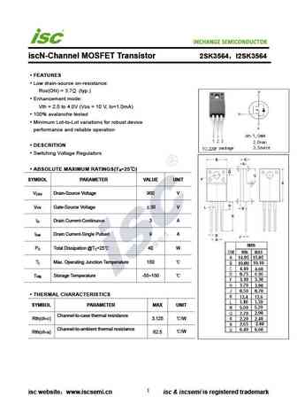
2sk3564.pdf

2SK3564 TOSHIBA Field Effect Transistor Silicon N Channel MOS Type ( -MOSIV) 2SK3564 Switching Regulator Applications Unit mm Low drain-source ON resistance RDS (ON) = 3.7 (typ.) High forward transfer admittance Yfs = 2.6 S (typ.) Low leakage current IDSS = 100 A (VDS = 720 V) Enhancement mode Vth = 2.0 4.0 V (VDS = 10 V, ID = 1 mA) Absolute Maximum... See More ⇒
8.6. Size:348K toshiba
2sk3563.pdf
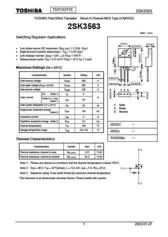
TENTATIVE 2SK3563 TOSHIBA Field Effect Transistor Silicon N Channel MOS Type ( -MOS ) 2SK3563 unit Switching Regulator Applications 10 0.3 2.7 0.2 3.2 0.2 Low drain-source ON resistance RDS (ON) = 1.35 (typ.) High forward transfer admittance Yfs = 3.5S (typ.) Low leakage current IDSS = 100 A (VDS = 500 V) Enhancement-mode Vth = 2... See More ⇒
8.7. Size:245K toshiba
2sk3568.pdf
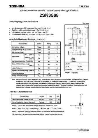
2SK3568 TOSHIBA Field Effect Transistor Silicon N Channel MOS Type ( -MOSVI) 2SK3568 Switching Regulator Applications Unit mm Low drain-source ON resistance RDS (ON) = 0.4 (typ.) High forward transfer admittance Yfs = 8.5S (typ.) Low leakage current IDSS = 100 A (VDS = 500 V) Enhancement mode Vth = 2.0 4.0 V (VDS = 10 V, ID = 1 mA) Absolute Maximum ... See More ⇒
8.8. Size:232K toshiba
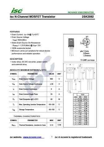
2sk3562.pdf

2SK3562 TOSHIBA Field Effect Transistor Silicon N Channel MOS Type ( -MOSVI) 2SK3562 Switching Regulator Applications Unit mm Low drain-source ON resistance RDS (ON) = 0.9 (typ.) High forward transfer admittance Yfs = 5.0S (typ.) Low leakage current IDSS = 100 A (VDS = 600 V) Enhancement mode Vth = 2.0 4.0 V (VDS = 10 V, ID = 1 mA) Maximum Ratings (... See More ⇒
8.10. Size:76K panasonic
2sk3560.pdf
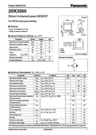
Power MOSFETs 2SK3560 Silicon N-channel power MOSFET Unit mm 4.6 0.2 10.5 0.3 1.4 0.1 For PDP/For high-speed switching Features Low on-resistance, low Qg 1.4 0.1 High avalanche resistance 2.5 0.2 0.8 0.1 2.54 0.3 0 to 0.3 Absolute Maximum Ratings TC = 25 C (10.2) Parameter Symbol Rating Unit (8.9) Drain-source surrender voltage VDSS 230 V 1 2 3 Gat... See More ⇒
8.11. Size:225K inchange semiconductor
2sk3566.pdf
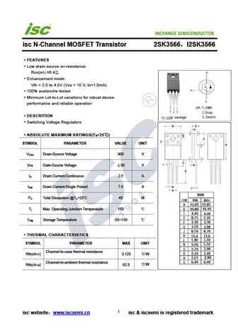
isc N-Channel MOSFET Transistor 2SK3566 I2SK3566 FEATURES Low drain-source on-resistance RDS(on) 6.4 . Enhancement mode Vth = 2.0 to 4.0V (VDS = 10 V, ID=1.0mA) 100% avalanche tested Minimum Lot-to-Lot variations for robust device performance and reliable operation DESCRITION Switching Voltage Regulators ABSOLUTE MAXIMUM RATINGS(T =25 ) a SYMBOL PARAMETER... See More ⇒
8.12. Size:237K inchange semiconductor
2sk3565.pdf
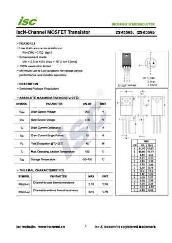
iscN-Channel MOSFET Transistor 2SK3565 I2SK3565 FEATURES Low drain-source on-resistance RDS(ON) =2.0 (typ.) Enhancement mode Vth = 2.0 to 4.0V (VDS = 10 V, ID=1.0mA) 100% avalanche tested Minimum Lot-to-Lot variations for robust device performance and reliable operation DESCRITION Switching Voltage Regulators ABSOLUTE MAXIMUM RATINGS(T =25 ) a SYMBOL PARAME... See More ⇒
8.13. Size:214K inchange semiconductor
2sk3569.pdf
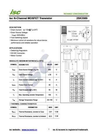
isc N-Channel MOSFET Transistor 2SK3569 DESCRIPTION Drain Current I = 10A@ T =25 D C Drain Source Voltage- V = 600V(Min) DSS Fast Switching Speed Minimum Lot-to-Lot variations for robust device performance and reliable operation APPLICATIONS Switching Regulators DC-DC Converter, Motor Control ABSOLUTE MAXIMUM RATINGS(T =25 ) a SYMBOL ARAMETER VALUE UNIT V D... See More ⇒
8.14. Size:279K inchange semiconductor
2sk3561.pdf
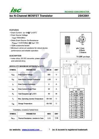
isc N-Channel MOSFET Transistor 2SK3561 FEATURES Drain Current I = 8A@ T =25 D C Drain Source Voltage V = 500V(Min) DSS Static Drain-Source On-Resistance R = 0.85 (Max) @ V = 10V DS(on) GS 100% avalanche tested Minimum Lot-to-Lot variations for robust device performance and reliable operation DESCRIPTION motor drive, DC-DC converter, power switch and solenoi... See More ⇒
8.15. Size:236K inchange semiconductor
2sk3564.pdf
iscN-Channel MOSFET Transistor 2SK3564 I2SK3564 FEATURES Low drain-source on-resistance RDS(ON) = 3.7 (typ.) Enhancement mode Vth = 2.0 to 4.0V (VDS = 10 V, ID=1.0mA) 100% avalanche tested Minimum Lot-to-Lot variations for robust device performance and reliable operation DESCRITION Switching Voltage Regulators ABSOLUTE MAXIMUM RATINGS(T =25 ) a SYMBOL PARAM... See More ⇒
8.16. Size:279K inchange semiconductor
2sk3563.pdf

isc N-Channel MOSFET Transistor 2SK3563 FEATURES Drain Current I = 5A@ T =25 D C Drain Source Voltage V = 500V(Min) DSS Static Drain-Source On-Resistance R = 1.5 (Max) @ V = 10V DS(on) GS 100% avalanche tested Minimum Lot-to-Lot variations for robust device performance and reliable operation DESCRIPTION motor drive, DC-DC converter, power switch and solenoid... See More ⇒
8.17. Size:253K inchange semiconductor
2sk3568.pdf
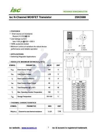
isc N-Channel MOSFET Transistor 2SK3568 FEATURES Drain-source on-resistance RDS(on) 0.52 @10V Low leakage current IDSS ... See More ⇒
8.18. Size:279K inchange semiconductor
2sk3562.pdf
isc N-Channel MOSFET Transistor 2SK3562 FEATURES Drain Current I = 6A@ T =25 D C Drain Source Voltage V = 600V(Min) DSS Static Drain-Source On-Resistance R = 1.25 (Max) @ V = 10V DS(on) GS 100% avalanche tested Minimum Lot-to-Lot variations for robust device performance and reliable operation DESCRIPTION motor drive, DC-DC converter, power switch and solenoi... See More ⇒
Detailed specifications: 2SK3462, 2SK3497, 2SK3499, 2SK3506, 2SK3543, 2SK3561, 2SK3562, 2SK3563, IRF540, 2SK3568, 2SK3569, 2SK3625, 2SK3662, 2SK3667, 2SK3669, 2SK3797, 2SK3844
Keywords - 2SK3567 MOSFET specs
2SK3567 cross reference
2SK3567 equivalent finder
2SK3567 pdf lookup
2SK3567 substitution
2SK3567 replacement
Can't find your MOSFET?
Learn how to find a substitute transistor by analyzing voltage, current and package compatibility