BUZ11 Specs and Replacement
Type Designator: BUZ11
Type of Transistor: MOSFET
Type of Control Channel: N
-Channel
Absolute Maximum Ratings
Pd ⓘ
- Maximum Power Dissipation: 120
W
|Vds|ⓘ - Maximum Drain-Source Voltage: 50
V
|Vgs|ⓘ - Maximum Gate-Source Voltage: 20
V
|Id| ⓘ - Maximum Drain Current: 36
A
Tj ⓘ - Maximum Junction Temperature: 150
°C
Electrical Characteristics
Cossⓘ -
Output Capacitance: 1500
pF
Rds ⓘ - Maximum Drain-Source On-State Resistance: 0.04
Ohm
Package:
TO220
-
MOSFET ⓘ Cross-Reference Search
BUZ11 datasheet
..1. Size:173K st
buz11.pdf 
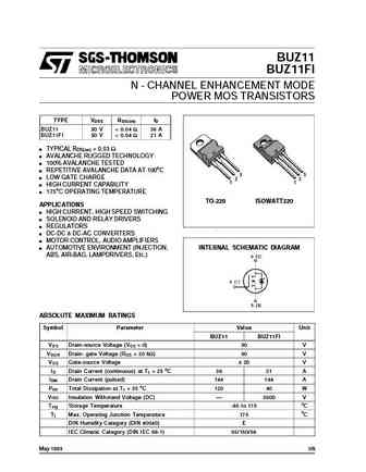
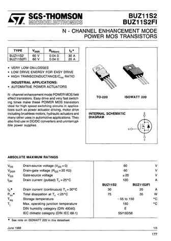
BUZ11 BUZ11FI N - CHANNEL ENHANCEMENT MODE POWER MOS TRANSISTORS TYPE V R I DSS DS(on) D BUZ11 50 V ... See More ⇒
..2. Size:81K fairchild semi
buz11.pdf
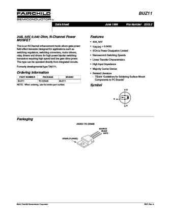
BUZ11 Data Sheet June 1999 File Number 2253.2 30A, 50V, 0.040 Ohm, N-Channel Power Features MOSFET 30A, 50V [ /Title This is an N-Channel enhancement mode silicon gate power rDS(ON) = 0.040 (BUZ1 field effect transistor designed for applications such as SOA is Power Dissipation Limited 1) switching regulators, switching converters, motor drivers, Nanosecond Sw... See More ⇒
..3. Size:218K onsemi
buz11.pdf
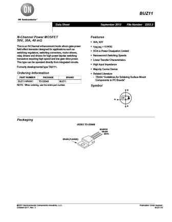
BUZ11 Data Sheet September 2013 File Number 2253.2 Features N-Channel Power MOSFET 50V, 30A, 40 m 30A, 50V This is an N-Channel enhancement mode silicon gate power rDS(ON) = 0.040 field effect transistor designed for applications such as SOA is Power Dissipation Limited switching regulators, switching converters, motor drivers, Nanosecond Switching Speeds re... See More ⇒
..4. Size:228K inchange semiconductor
buz11.pdf
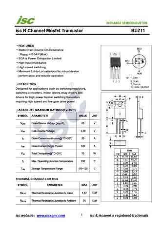
isc N-Channel Mosfet Transistor BUZ11 FEATURES Static Drain-Source On-Resistance R = 0.04 (Max) DS(on) SOA is Power Dissipation Limited High input impedance High speed switching Minimum Lot-to-Lot variations for robust device performance and reliable operation DESCRITION Designed for applications such as switching regulators, switching converters, motor drivers,rela... See More ⇒
0.1. Size:116K st
buz11a.pdf
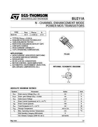
BUZ11A N - CHANNEL ENHANCEMENT MODE POWER MOS TRANSISTORS TYPE V R I DSS DS(on) D BUZ11A 50 V ... See More ⇒
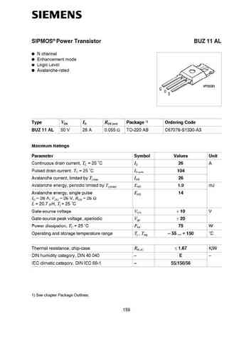
0.4. Size:88K siemens
buz110s spp80n05.pdf
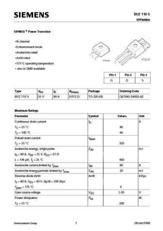
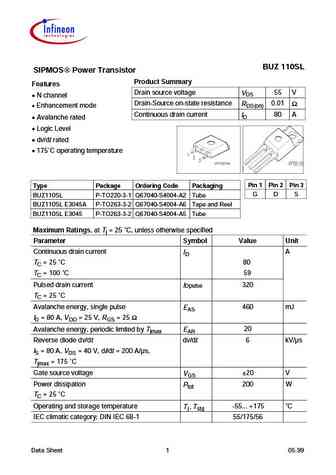
BUZ 110 S SPP80N05 SIPMOS Power Transistor N channel Enhancement mode Avalanche-rated dv/dt rated 175 C operating temperature also in SMD available Pin 1 Pin 2 Pin 3 G D S Type VDS ID RDS(on) Package Ordering Code BUZ 110 S 55 V 80 A 0.012 TO-220 AB Q67040-S4005-A2 Maximum Ratings Parameter Symbol Values Unit Continuous drain current ID A TC = 25 ... See More ⇒
0.5. Size:77K siemens
buz111sl spp80n05l.pdf
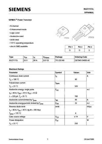
BUZ111SL SPP80N05L SIPMOS Power Transistor N channel Enhancement mode Logic Level Avalanche-rated dv/dt rated 175 C operating temperature also in SMD available Pin 1 Pin 2 Pin 3 G D S Type VDS ID RDS(on) Package Ordering Code BUZ111SL 55 V 80 A 0.01 TO-220 AB Q67040-S4003-A2 Maximum Ratings Parameter Symbol Values Unit Continuous drain current... See More ⇒
0.6. Size:126K infineon
buz110s.pdf
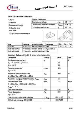
BUZ 110S SIPMOS Power Transistor Product Summary Features Drain source voltage 55 V VDS N channel Drain-Source on-state resistance 0.01 RDS(on) Enhancement mode Continuous drain current 80 A ID Avalanche rated dv/dt rated 175 C operating temperature Pin 1 Pin 2 Pin 3 Type Package Ordering Code Packaging G D S BUZ110S P-TO220-3-1 Q67040-S4005-A2 Tub... See More ⇒
0.7. Size:112K infineon
buz111s.pdf
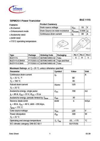
BUZ 111S SIPMOS Power Transistor Product Summary Features Drain source voltage 55 V VDS N channel Drain-Source on-state resistance 0.008 RDS(on) Enhancement mode Continuous drain current 80 A ID Avalanche rated dv/dt rated 175 C operating temperature Pin 1 Pin 2 Pin 3 Type Package Ordering Code Packaging G D S BUZ111S P-TO220-3-1 Q67040-S4003-A2 Tub... See More ⇒
0.8. Size:104K infineon
buz110sl.pdf
BUZ 110SL SIPMOS Power Transistor Product Summary Features Drain source voltage 55 V VDS N channel Drain-Source on-state resistance 0.01 RDS(on) Enhancement mode Continuous drain current 80 A ID Avalanche rated Logic Level dv/dt rated 175 C operating temperature Pin 1 Pin 2 Pin 3 Type Package Ordering Code Packaging G D S BUZ110SL P-TO220-3-1 Q... See More ⇒
0.9. Size:101K infineon
buz111sl.pdf
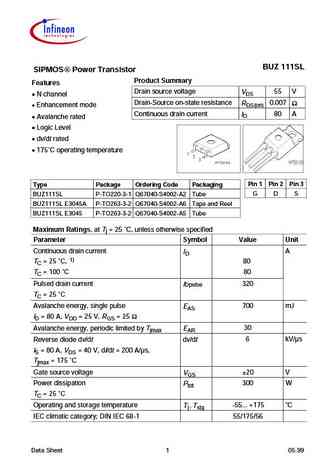
BUZ 111SL SIPMOS Power Transistor Product Summary Features Drain source voltage 55 V VDS N channel Drain-Source on-state resistance 0.007 RDS(on) Enhancement mode Continuous drain current 80 A ID Avalanche rated Logic Level dv/dt rated 175 C operating temperature Pin 1 Pin 2 Pin 3 Type Package Ordering Code Packaging G D S BUZ111SL P-TO220-3-1 ... See More ⇒
0.10. Size:229K inchange semiconductor
buz11a.pdf
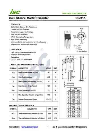
isc N-Channel Mosfet Transistor BUZ11A FEATURES Static Drain-Source On-Resistance R = 0.055 (Max) DS(on) Avalanche rugged technology High current capability 175 Operating Temperature High speed switching Minimum Lot-to-Lot variations for robust device performance and reliable operation DESCRITION High current,high speed switching Solenoid and relay drivers... See More ⇒
0.11. Size:229K inchange semiconductor
buz11s2.pdf
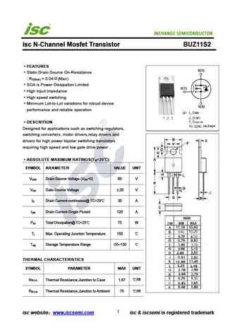
isc N-Channel Mosfet Transistor BUZ11S2 FEATURES Static Drain-Source On-Resistance R = 0.04 (Max) DS(on) SOA is Power Dissipation Limited High input impedance High speed switching Minimum Lot-to-Lot variations for robust device performance and reliable operation DESCRITION Designed for applications such as switching regulators, switching converters, motor drivers,re... See More ⇒
Detailed specifications: BUP66
, BUP67
, BUP68
, BUP69
, BUP70
, BUP71
, BUZ10
, BUZ10A
, IRF640
, BUZ11A
, BUZ11FI
, BUZ20
, BUZ21
, BUZ23
, BUZ24
, BUZ25
, BUZ32
.
Keywords - BUZ11 MOSFET specs
BUZ11 cross reference
BUZ11 equivalent finder
BUZ11 pdf lookup
BUZ11 substitution
BUZ11 replacement
Can't find your MOSFET?
Learn how to find a substitute transistor by analyzing voltage, current and package compatibility