SSF1331P Specs and Replacement
Type Designator: SSF1331P
Type of Transistor: MOSFET
Type of Control Channel: P-Channel
Absolute Maximum Ratings
Pd ⓘ - Maximum Power Dissipation: 0.34 W
|Vds|ⓘ - Maximum Drain-Source Voltage: 30 V
|Vgs|ⓘ - Maximum Gate-Source Voltage: 20 V
|Id| ⓘ - Maximum Drain Current: 1.5 A
Tj ⓘ - Maximum Junction Temperature: 150 °C
Electrical Characteristics
tr ⓘ - Rise Time: 9 nS
RDSonⓘ - Maximum Drain-Source On-State Resistance: 0.112 Ohm
Package: SOT323
SSF1331P substitution
- MOSFET ⓘ Cross-Reference Search
SSF1331P datasheet
ssf1331p.pdf
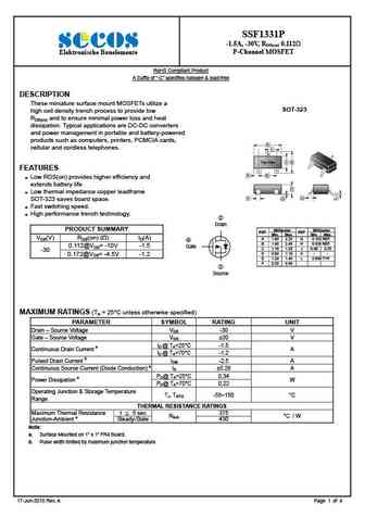
SSF1331P -1.5A, -30V, RDS(on) 0.112 P-Channel MOSFET Elektronische Bauelemente RoHS Compliant Product A Suffix of -C specifies halogen & lead-free DESCRIPTION These miniature surface mount MOSFETs utilize a SOT-323 high cell density trench process to provide low RDS(on) and to ensure minimal power loss and heat dissipation. Typical applications are DC-DC converters... See More ⇒
ssf1321p.pdf
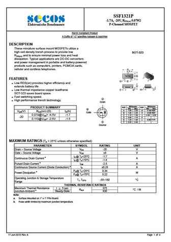
SSF1321P -1.7A, -20V, RDS(on) 0.079 P-Channel MOSFET Elektronische Bauelemente RoHS Compliant Product A Suffix of -C specifies halogen & lead-free DESCRIPTION These miniature surface mount MOSFETs utilize a high cell density trench process to provide low SOT-323 RDS(on) and to ensure minimal power loss and heat dissipation. Typical applications are DC-DC converters... See More ⇒
ssf1320n.pdf
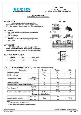
SSF1320N 2A , 20V , RDS(ON) 58 m N-Channel Enhancement Mode MOSFET Elektronische Bauelemente RoHS Compliant Product A suffix of -C specifies halogen and lead-free DESCRIPTION SOT-323 These miniature surface mount MOSFETs A utilize a high cell density trench process to provide low L 3 RDS(ON) and to ensure minimal power loss and heat dissipation. ... See More ⇒
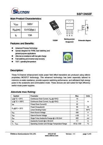
ssf13n50.pdf
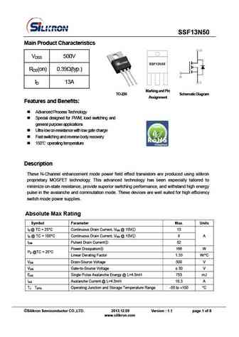
SSF13N50 Main Product Characteristics VDSS 500V RDS(on) 0.39 (typ.) ID 13A Marking and Pin TO-220 Schematic Diagram Assignment Features and Benefits Advanced Process Technology Special designed for PWM, load switching and general purpose applications Ultra low on-resistance with low gate charge Fast switching and reverse body recovery 150 o... See More ⇒
Detailed specifications: SSE90N04-03P, SSE90N06-10P, SSE90N06-30P, SSE90N08-08, SSE90N10-14, SSE90P06-08P, SSF1320N, SSF1321P, IRF540N, SSF7400, SSF7401, SSF84W, SSG0410, SSG4224, SSG4228, SSG4362N, SSG4390N
Keywords - SSF1331P MOSFET specs
SSF1331P cross reference
SSF1331P equivalent finder
SSF1331P pdf lookup
SSF1331P substitution
SSF1331P replacement
Need a MOSFET replacement? Our guide shows you how to find a perfect substitute by comparing key parameters and specs
History: LNE08R085 | MTH8N35
🌐 : EN ES РУ

LIST
Last Update
MOSFET: AUN084N10 | AUN065N10 | AUN063N10 | AUN062N08BG | AUN060N08AG | AUN053N10 | AUN050N08BGL | AUN045N085 | AUN042N055 | AUN036N10
Popular searches
2n4240 | 2n5210 transistor | toshiba 2sc2290 | pk6d0ba mosfet | 2sd726 | c536 transistor equivalent | 2sa1294 datasheet | mp10b transistor