SSF1331P. Аналоги и основные параметры
Наименование производителя: SSF1331P
Тип транзистора: MOSFET
Полярность: P
Предельные значения
Pd ⓘ - Максимальная рассеиваемая мощность: 0.34 W
|Vds|ⓘ - Максимально допустимое напряжение сток-исток: 30 V
|Vgs|ⓘ - Максимально допустимое напряжение затвор-исток: 20 V
|Id| ⓘ - Максимально допустимый постоянный ток стока: 1.5 A
Tj ⓘ - Максимальная температура канала: 150 °C
Электрические характеристики
tr ⓘ - Время нарастания: 9 ns
RDSonⓘ - Сопротивление сток-исток открытого транзистора: 0.112 Ohm
Тип корпуса: SOT323
Аналог (замена) для SSF1331P
- подборⓘ MOSFET транзистора по параметрам
SSF1331P даташит
ssf1331p.pdf
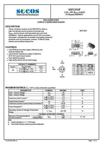
SSF1331P -1.5A, -30V, RDS(on) 0.112 P-Channel MOSFET Elektronische Bauelemente RoHS Compliant Product A Suffix of -C specifies halogen & lead-free DESCRIPTION These miniature surface mount MOSFETs utilize a SOT-323 high cell density trench process to provide low RDS(on) and to ensure minimal power loss and heat dissipation. Typical applications are DC-DC converters
ssf1321p.pdf
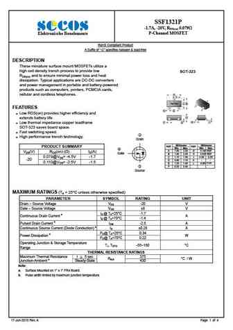
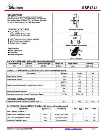
SSF1321P -1.7A, -20V, RDS(on) 0.079 P-Channel MOSFET Elektronische Bauelemente RoHS Compliant Product A Suffix of -C specifies halogen & lead-free DESCRIPTION These miniature surface mount MOSFETs utilize a high cell density trench process to provide low SOT-323 RDS(on) and to ensure minimal power loss and heat dissipation. Typical applications are DC-DC converters
ssf1320n.pdf
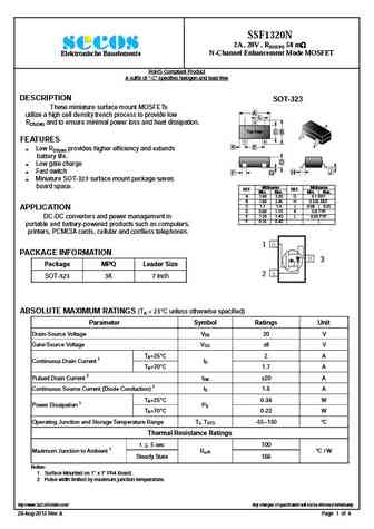
SSF1320N 2A , 20V , RDS(ON) 58 m N-Channel Enhancement Mode MOSFET Elektronische Bauelemente RoHS Compliant Product A suffix of -C specifies halogen and lead-free DESCRIPTION SOT-323 These miniature surface mount MOSFETs A utilize a high cell density trench process to provide low L 3 RDS(ON) and to ensure minimal power loss and heat dissipation.
ssf13n50.pdf
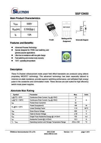
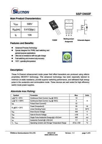
SSF13N50 Main Product Characteristics VDSS 500V RDS(on) 0.39 (typ.) ID 13A Marking and Pin TO-220 Schematic Diagram Assignment Features and Benefits Advanced Process Technology Special designed for PWM, load switching and general purpose applications Ultra low on-resistance with low gate charge Fast switching and reverse body recovery 150 o
Другие MOSFET... SSE90N04-03P , SSE90N06-10P , SSE90N06-30P , SSE90N08-08 , SSE90N10-14 , SSE90P06-08P , SSF1320N , SSF1321P , IRF540N , SSF7400 , SSF7401 , SSF84W , SSG0410 , SSG4224 , SSG4228 , SSG4362N , SSG4390N .
🌐 : EN ES РУ

Список транзисторов
Обновления
MOSFET: AUN084N10 | AUN065N10 | AUN063N10 | AUN062N08BG | AUN060N08AG | AUN053N10 | AUN050N08BGL | AUN045N085 | AUN042N055 | AUN036N10 | AUD069N10A | AUD062N08BG | AUD060N08AG | AUD060N055 | AUD056N08BGL | AUB062N08BG
Popular searches
2n4240 | 2n5210 transistor | toshiba 2sc2290 | pk6d0ba mosfet | 2sd726 | c536 transistor equivalent | 2sa1294 datasheet | mp10b transistor