FDC6303N Datasheet. Specs and Replacement
Type Designator: FDC6303N 📄📄
Type of Transistor: MOSFET
Type of Control Channel: N-Channel
Absolute Maximum Ratings
Pd ⓘ - Maximum Power Dissipation: 0.9 W
|Vds|ⓘ - Maximum Drain-Source Voltage: 25 V
|Vgs|ⓘ - Maximum Gate-Source Voltage: 8 V
|Id| ⓘ - Maximum Drain Current: 0.68 A
Tj ⓘ - Maximum Junction Temperature: 150 °C
Electrical Characteristics
tr ⓘ - Rise Time: 8.5 nS
Cossⓘ - Output Capacitance: 28 pF
RDSonⓘ - Maximum Drain-Source On-State Resistance: 0.45 Ohm
Package: SUPERSOT6
📄📄 Copy
- MOSFET ⓘ Cross-Reference Search
FDC6303N datasheet
..1. Size:78K fairchild semi
fdc6303n.pdf 
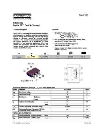
August 1997 FDC6303N Digital FET, Dual N-Channel General Description Features 25 V, 0.68 A continuous, 2 A Peak. These dual N-Channel logic level enhancement mode field RDS(ON) = 0.6 @ VGS = 2.7 V effect transistors are produced using Fairchild's proprietary, high cell density, DMOS technology. This very high density RDS(ON) = 0.45 @ VGS= 4.5 V. process is especially tailored... See More ⇒
8.1. Size:73K fairchild semi
fdc6305n.pdf
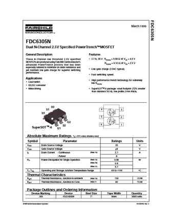
March 1999 FDC6305N Dual N-Channel 2.5V Specified PowerTrenchTM MOSFET General Description Features 2.7 A, 20 V. RDS(ON) = 0.08 @ VGS = 4.5 V These N-Channel low threshold 2.5V specified MOSFETs are produced using Fairchild Semiconductor's RDS(ON) = 0.12 @ VGS = 2.5 V advanced PowerTrench process that has been especially tailored to minimize on-state resistance and Low... See More ⇒
8.2. Size:61K fairchild semi
fdc6306p.pdf
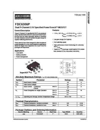
February 1999 FDC6306P Dual P-Channel 2.5V Specified PowerTrench MOSFET Features General Description These P-Channel 2.5V specified MOSFETs are produced -1.9 A, -20 V. RDS(on) = 0.170 @ VGS = -4.5 V using Fairchild Semiconductor's advanced PowerTrench RDS(on) = 0.250 @ VGS = -2.5 V process that has been especially tailored to minimize on-state resistance and yet maintain... See More ⇒
8.3. Size:80K fairchild semi
fdc6304p.pdf
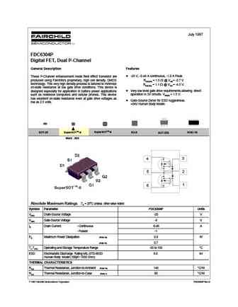
July 1997 FDC6304P Digital FET, Dual P-Channel General Description Features -25 V, -0.46 A continuous, -1.0 A Peak. These P-Channel enhancement mode field effect transistor are produced using Fairchild's proprietary, high cell density, DMOS RDS(ON) = 1.5 @ VGS= -2.7 V technology. This very high density process is tailored to minimize RDS(ON) = 1.1 @ VGS = -4.5 V. on-state ... See More ⇒
8.4. Size:82K fairchild semi
fdc6302p.pdf
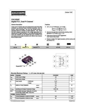
October 1997 FDC6302P Digital FET, Dual P-Channel General Description Features These Dual P-Channel logic level enhancement mode field effect -25 V, -0.12 A continuous, -0.5 A Peak. transistors are produced using Fairchild's proprietary, high cell RDS(ON) = 13 @ VGS= -2.7 V density, DMOS technology. This very high density process is RDS(ON) = 10 @ VGS = -4.5 V. especially... See More ⇒
8.5. Size:374K fairchild semi
fdc6301n.pdf
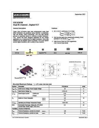
September 2001 FDC6301N Dual N-Channel , Digital FET General Description Features 25 V, 0.22 A continuous, 0.5 A Peak. These dual N-Channel logic level enhancement mode field effect transistors are produced using Fairchild 's proprietary, RDS(ON) = 5 @ VGS= 2.7 V high cell density, DMOS technology. This very high density RDS(ON) = 4 @ VGS= 4.5 V. process is especially tailo... See More ⇒
8.6. Size:150K fairchild semi
fdc6308p.pdf
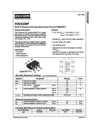
July 1999 FDC6308P Dual P-Channel 2.5V Specified PowerTrenchTM MOSFET General Description Features This P-Channel 2.5V specified MOSFET is a rugged -1.7 A, -18 V. RDS(ON) = 0.18 @ VGS = -4.5 V gate version of Fairchild Semiconductor's advanced RDS(ON) = 0.30 @ VGS = -2.5 V PowerTrench process. It has been optimized for power management applications with a wide range of gate ... See More ⇒
8.7. Size:185K onsemi
fdc6305n.pdf

Is Now Part of To learn more about ON Semiconductor, please visit our website at www.onsemi.com Please note As part of the Fairchild Semiconductor integration, some of the Fairchild orderable part numbers will need to change in order to meet ON Semiconductor s system requirements. Since the ON Semiconductor product management systems do not have the ability to manage part nomenclatur... See More ⇒
8.8. Size:175K onsemi
fdc6306p.pdf

Is Now Part of To learn more about ON Semiconductor, please visit our website at www.onsemi.com Please note As part of the Fairchild Semiconductor integration, some of the Fairchild orderable part numbers will need to change in order to meet ON Semiconductor s system requirements. Since the ON Semiconductor product management systems do not have the ability to manage part nomenclatur... See More ⇒
8.9. Size:604K onsemi
fdc6301n.pdf
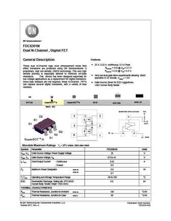
FDC6301N Dual N-Channel , Digital FET Features General Description 25 V, 0.22 A continuous, 0.5 A Peak. These dual N-Channel logic level enhancement mode field RDS(ON) = 5 @ VGS= 2.7 V effect transistors are produced using ON Semiconductor 's RDS(ON) = 4 @ VGS= 4.5 V. proprietary, high cell density, DMOS technology. This very high density process is especially tailored to... See More ⇒
8.10. Size:2356K cn vbsemi
fdc6305n.pdf
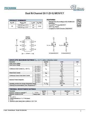
FDC6305N www.VBsemi.tw Dual N-Channel 20 V (D-S) MOSFET FEATURES PRODUCT SUMMARY Halogen-free According to IEC 61249-2-21 VDS (V) RDS(on) ( ) ID (A)a Qg (Typ.) Definition 0.022 at VGS = 4.5 V TrenchFET Power MOSFET 6.0 20 1.8 nC 100 % Rg Tested 0.028 at VGS = 2.5 V 5.0 Compliant to RoHS Directive 2002/95/EC TSOP-6 D1 D 2 D Top View G1 D1 1 6 G 1 ... See More ⇒
Detailed specifications: FDB7030BL, FDB7030L, FDB7045L, FDB8030L, AS3401, FDC5612, FDC6301N, FDC6302P, IRFB3607, FDC6304P, FDC6305N, FDC6306P, FDC6308P, FDC633N, FDC634P, FDC636P, FDC637AN
Keywords - FDC6303N MOSFET specs
FDC6303N cross reference
FDC6303N equivalent finder
FDC6303N pdf lookup
FDC6303N substitution
FDC6303N replacement
Learn how to find the right MOSFET substitute. A guide to cross-reference, check specs and replace MOSFETs in your circuits.
