FDC6303N datasheet, аналоги, основные параметры
Наименование производителя: FDC6303N 📄📄
Тип транзистора: MOSFET
Полярность: N
Предельные значения
Pd ⓘ - Максимальная рассеиваемая мощность: 0.9 W
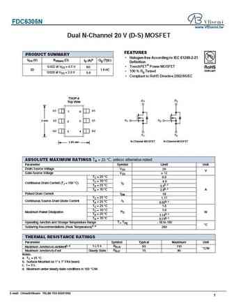
|Vds|ⓘ - Максимально допустимое напряжение сток-исток: 25 V
|Vgs|ⓘ - Максимально допустимое напряжение затвор-исток: 8 V
|Id| ⓘ - Максимально допустимый постоянный ток стока: 0.68 A
Tj ⓘ - Максимальная температура канала: 150 °C
Электрические характеристики
tr ⓘ - Время нарастания: 8.5 ns
Cossⓘ - Выходная емкость: 28 pf
RDSonⓘ - Сопротивление сток-исток открытого транзистора: 0.45 Ohm
Тип корпуса: SUPERSOT6
📄📄 Копировать
Аналог (замена) для FDC6303N
- подборⓘ MOSFET транзистора по параметрам
FDC6303N даташит
fdc6303n.pdf
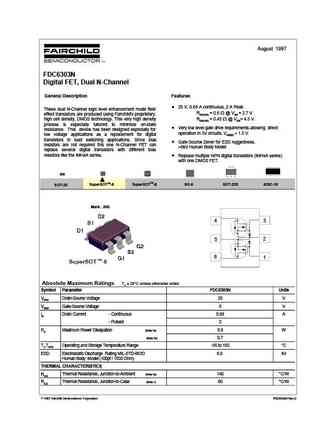
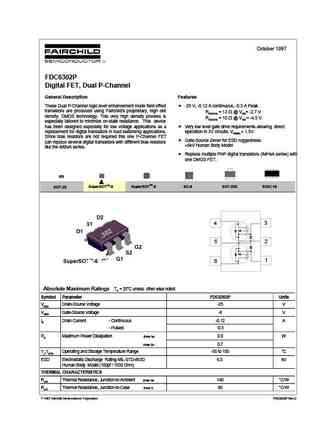
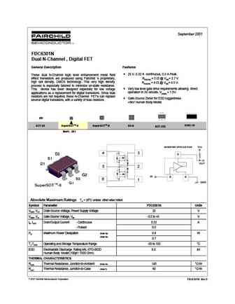
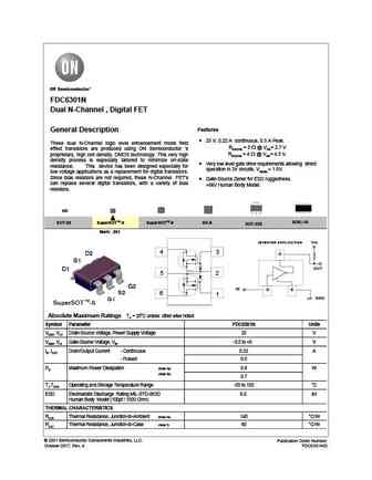
August 1997 FDC6303N Digital FET, Dual N-Channel General Description Features 25 V, 0.68 A continuous, 2 A Peak. These dual N-Channel logic level enhancement mode field RDS(ON) = 0.6 @ VGS = 2.7 V effect transistors are produced using Fairchild's proprietary, high cell density, DMOS technology. This very high density RDS(ON) = 0.45 @ VGS= 4.5 V. process is especially tailored
fdc6305n.pdf
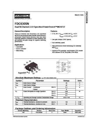
March 1999 FDC6305N Dual N-Channel 2.5V Specified PowerTrenchTM MOSFET General Description Features 2.7 A, 20 V. RDS(ON) = 0.08 @ VGS = 4.5 V These N-Channel low threshold 2.5V specified MOSFETs are produced using Fairchild Semiconductor's RDS(ON) = 0.12 @ VGS = 2.5 V advanced PowerTrench process that has been especially tailored to minimize on-state resistance and Low
fdc6306p.pdf
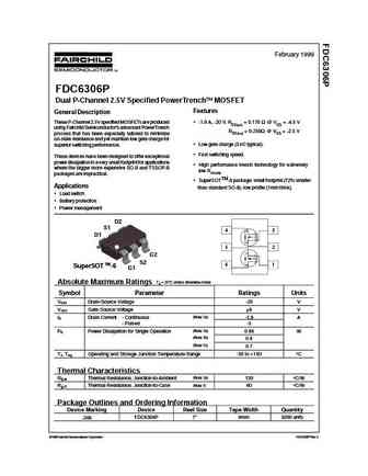
February 1999 FDC6306P Dual P-Channel 2.5V Specified PowerTrench MOSFET Features General Description These P-Channel 2.5V specified MOSFETs are produced -1.9 A, -20 V. RDS(on) = 0.170 @ VGS = -4.5 V using Fairchild Semiconductor's advanced PowerTrench RDS(on) = 0.250 @ VGS = -2.5 V process that has been especially tailored to minimize on-state resistance and yet maintain
fdc6304p.pdf
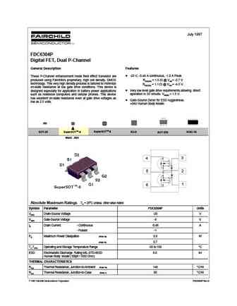
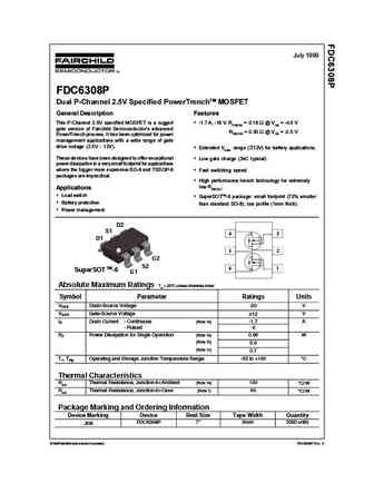
July 1997 FDC6304P Digital FET, Dual P-Channel General Description Features -25 V, -0.46 A continuous, -1.0 A Peak. These P-Channel enhancement mode field effect transistor are produced using Fairchild's proprietary, high cell density, DMOS RDS(ON) = 1.5 @ VGS= -2.7 V technology. This very high density process is tailored to minimize RDS(ON) = 1.1 @ VGS = -4.5 V. on-state


Другие IGBT... FDB7030BL, FDB7030L, FDB7045L, FDB8030L, AS3401, FDC5612, FDC6301N, FDC6302P, IRFB3607, FDC6304P, FDC6305N, FDC6306P, FDC6308P, FDC633N, FDC634P, FDC636P, FDC637AN
Параметры MOSFET. Взаимосвязь и компромиссы
History: HSS2300A
🌐 : EN ES РУ

Список транзисторов
Обновления
MOSFET: BLM3404 | BL4N90 | SI2309S | SI2301F | BMSN3139 | BMS2302 | BMS2301 | BMDFN2302 | BMDFN2301 | BM8205 | BM3139KT | BM3134KE | BM3134E | AO3415E | AO3401F | CS65N25AKR
Popular searches
2sc3281 datasheet | 2sa1106 | 2sb56 | 2sc1451 datasheet | 2sc373 | a1023 datasheet | 2sc1080 | 2sb618