CEB12N6 Specs and Replacement
Type Designator: CEB12N6
Type of Transistor: MOSFET
Type of Control Channel: N-Channel
Absolute Maximum Ratings
Pd ⓘ - Maximum Power Dissipation: 250 W
|Vds|ⓘ - Maximum Drain-Source Voltage: 600 V
|Vgs|ⓘ - Maximum Gate-Source Voltage: 30 V
|Id| ⓘ - Maximum Drain Current: 12 A
Tj ⓘ - Maximum Junction Temperature: 175 °C
Electrical Characteristics
tr ⓘ - Rise Time: 58 nS
Cossⓘ - Output Capacitance: 220 pF
RDSonⓘ - Maximum Drain-Source On-State Resistance: 0.65 Ohm
Package: TO263
CEB12N6 substitution
- MOSFET ⓘ Cross-Reference Search
CEB12N6 datasheet
cep12n6 ceb12n6 cef12n6.pdf

CEP12N6/CEB12N6 CEF12N6 PRELIMINARY N-Channel Enhancement Mode Field Effect Transistor FEATURES Type VDSS RDS(ON) ID @VGS CEP12N6 600V 0.65 12A 10V CEB12N6 600V 0.65 12A 10V CEF12N6 600V 0.65 12A d 10V D Super high dense cell design for extremely low RDS(ON). High power and current handing capability. Lead free product is acquired. G S CEB SERIES CEP SERIES CEF SERIES ... See More ⇒
cep12n65 ceb12n65 cef12n65.pdf
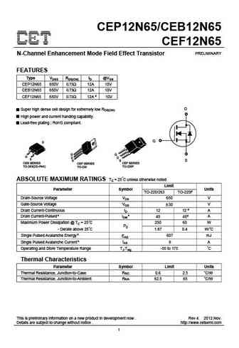
CEP12N65/CEB12N65 CEF12N65 PRELIMINARY N-Channel Enhancement Mode Field Effect Transistor FEATURES Type VDSS RDS(ON) ID @VGS CEP12N65 650V 0.73 12A 10V CEB12N65 650V 0.73 12A 10V CEF12N65 650V 0.73 12A d 10V D Super high dense cell design for extremely low RDS(ON). High power and current handing capability. Lead-free plating ; RoHS compliant. G S CEB SERIES CEP SERIES C... See More ⇒
cep12n5 ceb12n5 cef12n5.pdf
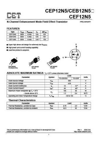
CEP12N5/CEB12N5 CEF12N5 PRELIMINARY N-Channel Enhancement Mode Field Effect Transistor FEATURES Type VDSS RDS(ON) ID @VGS CEP12N5 500V 0.54 12A 10V CEB12N5 500V 0.54 12A 10V CEF12N5 500V 0.54 12A d 10V D Super high dense cell design for extremely low RDS(ON). High power and current handing capability. Lead free product is acquired. G S CEB SERIES CEP SERIES CEF SERIES ... See More ⇒
cep12p10 ceb12p10.pdf
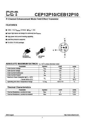
CEP12P10/CEB12P10 P-Channel Enhancement Mode Field Effect Transistor FEATURES -100V, -11A, RDS(ON) =315m @VGS = -10V. Super high dense cell design for extremely low RDS(ON). High power and current handing capability. D Lead free product is acquired. TO-220 & TO-263 package. G CEB SERIES CEP SERIES TO-263(DD-PAK) S TO-220 ABSOLUTE MAXIMUM RATINGS Tc = 25 C unless otherwise noted... See More ⇒
Detailed specifications: CEF14N5, CEP14N5, CEB13N5, CEP13N5, CEB12N5, CEF12N5, CEF13N5, CEP12N5, IRF1405, CEF12N6, CEP12N6, CEP10N4, CEB10N4, CEI10N4, CEF10N4, CEB10N6, CEF10N6
Keywords - CEB12N6 MOSFET specs
CEB12N6 cross reference
CEB12N6 equivalent finder
CEB12N6 pdf lookup
CEB12N6 substitution
CEB12N6 replacement
Need a MOSFET replacement? Our guide shows you how to find a perfect substitute by comparing key parameters and specs
🌐 : EN ES РУ

LIST
Last Update
MOSFET: AKF30N5P0SX | AKF30N10S | AKF20P45D | CM4407 | CM3407 | CM3400 | SVF11N65F | SVF11N65T | FKBB3105 | EHBA036R1
Popular searches
irf9530 datasheet | mj21194 | oc71 transistor | 2n3440 | bc550c | 2n3904 transistor datasheet | p75nf75 | d880 transistor