CED01N6G Specs and Replacement
Type Designator: CED01N6G
Type of Transistor: MOSFET
Type of Control Channel: N-Channel
Absolute Maximum Ratings
Pd ⓘ - Maximum Power Dissipation: 31 W
|Vds|ⓘ - Maximum Drain-Source Voltage: 600 V
|Vgs|ⓘ - Maximum Gate-Source Voltage: 30 V
|Id| ⓘ - Maximum Drain Current: 1 A
Tj ⓘ - Maximum Junction Temperature: 150 °C
Electrical Characteristics
tr ⓘ - Rise Time: 11 nS
Cossⓘ - Output Capacitance: 55 pF
RDSonⓘ - Maximum Drain-Source On-State Resistance: 9.3 Ohm
Package: TO251
CED01N6G substitution
- MOSFET ⓘ Cross-Reference Search
CED01N6G datasheet
ced01n6g ceu01n6g.pdf
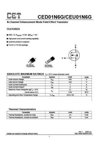
CED01N6G/CEU01N6G N-Channel Enhancement Mode Field Effect Transistor FEATURES 600V, 1A, RDS(ON) = 9.3 @VGS = 10V. High power and current handing capability. Lead free product is acquired. TO-251 & TO-252 package. D G D G S CEU SERIES CED SERIES TO-252(D-PAK) TO-251(I-PAK) S ABSOLUTE MAXIMUM RATINGS Tc = 25 C unless otherwise noted Parameter Symbol Limit Units Drain-Source ... See More ⇒
ceu01n65a ced01n65a.pdf
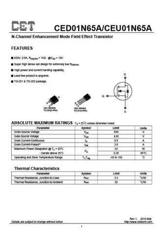
CED01N65A/CEU01N65A N-Channel Enhancement Mode Field Effect Transistor FEATURES 650V, 0.9A, RDS(ON) = 15 @VGS = 10V. Super high dense cell design for extremely low RDS(ON). High power and current handing capability. D Lead free product is acquired. TO-251 & TO-252 package. G D G S CEU SERIES CED SERIES TO-252(D-PAK) TO-251(I-PAK) S ABSOLUTE MAXIMUM RATINGS Tc = 25 C unless ... See More ⇒
ceu01n65 ced01n65.pdf
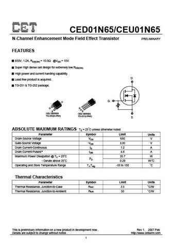
CED01N65/CEU01N65 N-Channel Enhancement Mode Field Effect Transistor PRELIMINARY FEATURES 650V, 1.2A, RDS(ON) = 10.5 @VGS = 10V. Super high dense cell design for extremely low RDS(ON). High power and current handing capability. D Lead free product is acquired. TO-251 & TO-252 package. G D G S CEU SERIES CED SERIES TO-252(D-PAK) TO-251(I-PAK) S ABSOLUTE MAXIMUM RATINGS Tc = ... See More ⇒
ced01n7 ceu01n7.pdf
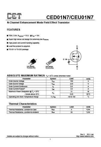
CED01N7/CEU01N7 N-Channel Enhancement Mode Field Effect Transistor FEATURES 700V, 0.8A, RDS(ON) = 18 @VGS = 10V. Super high dense cell design for extremely low RDS(ON). High power and current handing capability. Lead free product is acquired. D TO-251 & TO-252 package. G D G S CEU SERIES CED SERIES TO-252(D-PAK) TO-251(I-PAK) S ABSOLUTE MAXIMUM RATINGS Tc = 25 C unless othe... See More ⇒
Detailed specifications: CEP85N75, CEP85N75V, CEP9060N, CEP93A3, CEBF634, CEBF640, CED01N65, CED01N65A, IRF740, CED01N7, CED02N65A, CED02N65G, CED02N6A, CED02N6G, CED02N7G, CED02N7G-1, CED02N9
Keywords - CED01N6G MOSFET specs
CED01N6G cross reference
CED01N6G equivalent finder
CED01N6G pdf lookup
CED01N6G substitution
CED01N6G replacement
Can't find your MOSFET? Learn how to find a substitute transistor by analyzing voltage, current and package compatibility
