CED02N7G-1 Specs and Replacement
Type Designator: CED02N7G-1
Type of Transistor: MOSFET
Type of Control Channel: N-Channel
Absolute Maximum Ratings
Pd ⓘ - Maximum Power Dissipation: 48 W
|Vds|ⓘ - Maximum Drain-Source Voltage: 720 V
|Vgs|ⓘ - Maximum Gate-Source Voltage: 30 V
|Id| ⓘ - Maximum Drain Current: 1.6 A
Tj ⓘ - Maximum Junction Temperature: 150 °C
Electrical Characteristics
tr ⓘ - Rise Time: 12.5 nS
Cossⓘ - Output Capacitance: 55 pF
RDSonⓘ - Maximum Drain-Source On-State Resistance: 6.75 Ohm
Package: TO251
CED02N7G-1 substitution
- MOSFET ⓘ Cross-Reference Search
CED02N7G-1 datasheet
ceu02n7g-1 ced02n7g-1.pdf
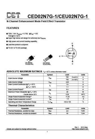
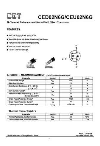
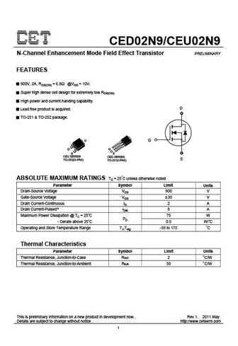
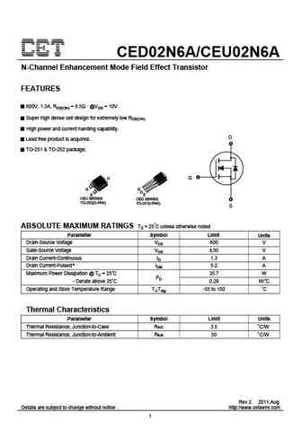
CED02N7G-1/CEU02N7G-1 N-Channel Enhancement Mode Field Effect Transistor FEATURES 720V, 1.6A, RDS(ON) = 6.75 @VGS = 10V. 750V@Tc=150 C Super high dense cell design for extremely low RDS(ON). High power and current handing capability. D Lead free product is acquired. TO-251 & TO-252 package. D G G S CEU SERIES CED SERIES S TO-252(D-PAK) TO-251(I-PAK) ABSOLUTE MAXIMUM RATING... See More ⇒
ceu02n7g ced02n7g.pdf
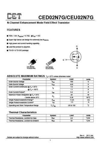
CED02N7G/CEU02N7G N-Channel Enhancement Mode Field Effect Transistor FEATURES 700V, 1.6A, RDS(ON) = 6.75 @VGS = 10V. Super high dense cell design for extremely low RDS(ON). High power and current handing capability. D Lead free product is acquired. TO-251 & TO-252 package. D G G S CEU SERIES CED SERIES S TO-252(D-PAK) TO-251(I-PAK) ABSOLUTE MAXIMUM RATINGS Tc = 25 C unless o... See More ⇒
ceu02n65g ced02n65g.pdf
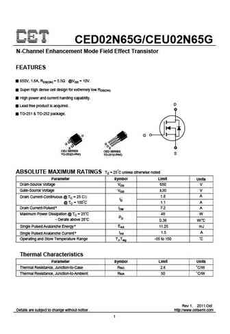
CED02N65G/CEU02N65G N-Channel Enhancement Mode Field Effect Transistor FEATURES 650V, 1.8A, RDS(ON) = 5.5 @VGS = 10V. Super high dense cell design for extremely low RDS(ON). High power and current handing capability. D Lead free product is acquired. TO-251 & TO-252 package. D G G S CEU SERIES CED SERIES S TO-252(D-PAK) TO-251(I-PAK) ABSOLUTE MAXIMUM RATINGS Tc = 25 C unless ... See More ⇒
ceu02n65a ced02n65a.pdf
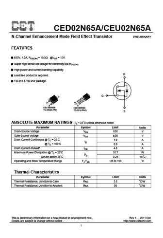
CED02N65A/CEU02N65A N-Channel Enhancement Mode Field Effect Transistor PRELIMINARY FEATURES 650V, 1.2A, RDS(ON) = 10.5 @VGS = 10V. Super high dense cell design for extremely low RDS(ON). High power and current handing capability. D Lead free product is acquired. TO-251 & TO-252 package. G D G S CEU SERIES CED SERIES TO-252(D-PAK) TO-251(I-PAK) S ABSOLUTE MAXIMUM RATINGS Tc ... See More ⇒
Detailed specifications: CED01N65A, CED01N6G, CED01N7, CED02N65A, CED02N65G, CED02N6A, CED02N6G, CED02N7G, IRFZ44, CED02N9, CED03N8, CED04N6, CED04N65, CED04N7G, CED05N65, CED06N7, CED07N65A
Keywords - CED02N7G-1 MOSFET specs
CED02N7G-1 cross reference
CED02N7G-1 equivalent finder
CED02N7G-1 pdf lookup
CED02N7G-1 substitution
CED02N7G-1 replacement
Need a MOSFET replacement? Our guide shows you how to find a perfect substitute by comparing key parameters and specs
History: BLP055N10-B | HM3413B
🌐 : EN ES РУ

LIST
Last Update
MOSFET: AKF30N5P0SX | AKF30N10S | AKF20P45D | CM4407 | CM3407 | CM3400 | SVF11N65F | SVF11N65T | FKBB3105 | EHBA036R1
Popular searches
bc239 transistor equivalent | 3sk41 | 2sc2240 transistor | c3198 | 2sc793 | 2sd313 replacement | 2n4249 | a1013 transistor