FDG315N Specs and Replacement
Type Designator: FDG315N
Type of Transistor: MOSFET
Type of Control Channel: N-Channel
Absolute Maximum Ratings
Pd ⓘ - Maximum Power Dissipation: 0.75 W
|Vds|ⓘ - Maximum Drain-Source Voltage: 30 V
|Vgs|ⓘ - Maximum Gate-Source Voltage: 20 V
|Id| ⓘ - Maximum Drain Current: 2 A
Tj ⓘ - Maximum Junction Temperature: 150 °C
Electrical Characteristics
tr ⓘ - Rise Time: 11 nS
Cossⓘ - Output Capacitance: 50 pF
RDSonⓘ - Maximum Drain-Source On-State Resistance: 0.12 Ohm
Package: SC70-6
FDG315N substitution
- MOSFET ⓘ Cross-Reference Search
FDG315N datasheet
fdg315n.pdf
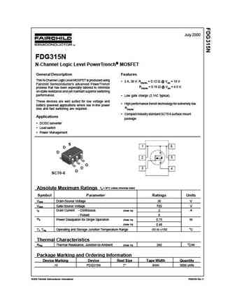
July 2000 FDG315N N-Channel Logic Level PowerTrench MOSFET General Description Features This N-Channel Logic Level MOSFET is produced using 2 A, 30 V. RDS(ON) = 0.12 @ VGS = 10 V Fairchild Semiconductor's advanced PowerTrench RDS(ON) = 0.16 @ VGS = 4.5 V. process that has been especially tailored to minimize on-state resistance and yet maintain super... See More ⇒
fdg313n d87z.pdf

July 2000 FDG313N Digital FET, N-Channel General Description Features This N-Channel enhancement mode field effect 0.95 A, 25 V. RDS(on) = 0.45 @ VGS = 4.5 V transistor is produced using Fairchild's proprietary, high RDS(on) = 0.60 @ VGS = 2.7 V. cell density, DMOS technology. This very high density process is especially tailored to minimize on-state resistance. This devic... See More ⇒
fdg311n.pdf
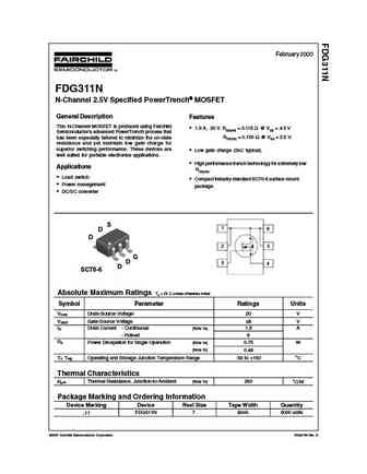
February 2000 FDG311N N-Channel 2.5V Specified PowerTrench MOSFET General Description Features This N-Channel MOSFET is produced using Fairchild 1.9 A, 20 V. RDS(ON) = 0.115 @ VGS = 4.5 V Semiconductor's advanced PowerTrench process that RDS(ON) = 0.150 @ VGS = 2.5 V. has been especially tailored to minimize the on-state resistance and yet maintain lo... See More ⇒
fdg313n.pdf
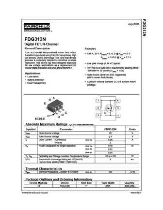
July 2000 FDG313N Digital FET, N-Channel General Description Features This N-Channel enhancement mode field effect 0.95 A, 25 V. RDS(on) = 0.45 @ VGS = 4.5 V transistor is produced using Fairchild's proprietary, high RDS(on) = 0.60 @ VGS = 2.7 V. cell density, DMOS technology. This very high density process is especially tailored to minimize on-state resistance. This devic... See More ⇒


Detailed specifications: FDD6680, FDD6680A, FDD6690A, AS3402, FDG311N, FDG312P, FDG313N, FDG314P, IRFB31N20D, FDG316P, FDG6301N, FDG6302P, FDG6303N, FDG6304P, FDN335N, FDN336P, FDN337N
Keywords - FDG315N MOSFET specs
FDG315N cross reference
FDG315N equivalent finder
FDG315N pdf lookup
FDG315N substitution
FDG315N replacement
Step-by-step guide to finding a MOSFET replacement. Cross-reference parts and ensure compatibility for your repair or project.
History: CS7N60CD
🌐 : EN ES РУ

LIST
Last Update
MOSFET: AUP060N055 | AUP056N10 | AUP056N08BGL | AUP052N085 | AUP045N12 | AUP039N10 | AUP034N10 | AUP034N06 | AUP033N08BG | AUP026N085
Popular searches
2sa1302 datasheet | mpsa13 transistor equivalent | кт817г характеристики | 2sc1972 | 2n5088 transistor equivalent | 2n5884 | bc640 | 2sc756