CEM6659 Specs and Replacement
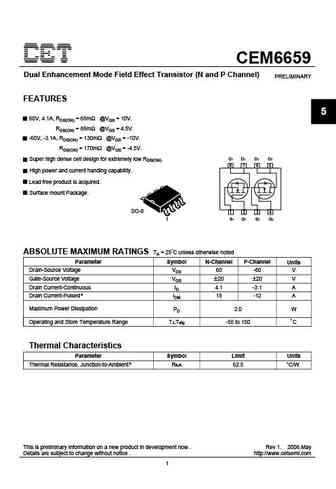
Type Designator: CEM6659
Type of Transistor: MOSFET
Type of Control Channel: NP-Channel
Absolute Maximum Ratings
Pd ⓘ - Maximum Power Dissipation: 2 W
|Vds|ⓘ - Maximum Drain-Source Voltage: 60 V
|Vgs|ⓘ - Maximum Gate-Source Voltage: 20 V
|Id| ⓘ - Maximum Drain Current: 4.1(3.1) A
Tj ⓘ - Maximum Junction Temperature: 150 °C
Electrical Characteristics
tr ⓘ - Rise Time: 3 nS
Cossⓘ - Output Capacitance: 80 pF
RDSonⓘ - Maximum Drain-Source On-State Resistance: 0.068 Ohm
Package: SO8
CEM6659 substitution
- MOSFET ⓘ Cross-Reference Search
CEM6659 datasheet
cem6659.pdf
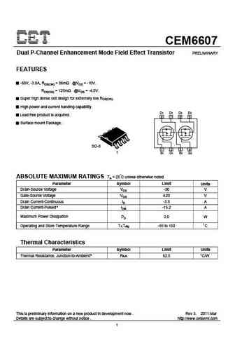
CEM6659 Dual Enhancement Mode Field Effect Transistor (N and P Channel) PRELIMINARY FEATURES 5 60V, 4.1A, RDS(ON) = 68m @VGS = 10V. RDS(ON) = 86m @VGS = 4.5V. -60V, -3.1A, RDS(ON) = 130m @VGS = -10V. RDS(ON) = 170m @VGS = -4.5V. D1 D1 D2 D2 Super high dense cell design for extremely low RDS(ON). 8 7 6 5 High power and current handing capability. Lead free product is a... See More ⇒
cem6659.pdf
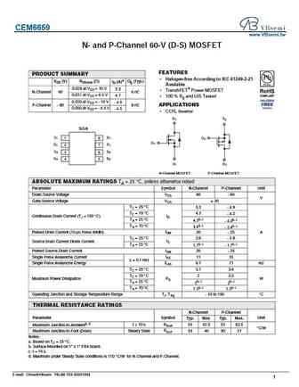
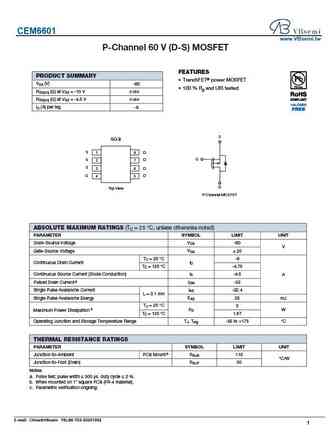
CEM6659 www.VBsemi.tw N- and P-Channel 60-V (D-S) MOSFET FEATURES PRODUCT SUMMARY Halogen-free According to IEC 61249-2-21 VDS (V) RDS(on) ( ) ID (A)a Qg (Typ.) Available 0.028 at VGS = 10 V 5.3 TrenchFET Power MOSFET N-Channel 60 6 nC 0.031 at VGS = 4.5 V 4.7 100 % Rg and UIS Tested 0.050 at VGS = - 10 V - 4.9 APPLICATIONS P-Channel - 60 8 nC 0.060 at VGS =... See More ⇒
cem6600.pdf
CEM6600 N-Channel Enhancement Mode Field Effect Transistor FEATURES 60V, 4A, RDS(ON) = 76m @VGS = 10V. RDS(ON) = 100m @VGS = 4.5V. Super high dense cell design for extremely low RDS(ON). High power and current handing capability. D D D D Lead free product is acquired. 8 7 6 5 Surface mount Package. SO-8 1 2 3 4 1 S S S G ABSOLUTE MAXIMUM RATINGS TA = 25 C unless otherwise... See More ⇒
cem6608.pdf
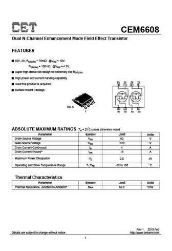
CEM6608 Dual N-Channel Enhancement Mode Field Effect Transistor FEATURES 60V, 4A, RDS(ON) = 76m @VGS = 10V. RDS(ON) = 100m @VGS = 4.5V. Super high dense cell design for extremely low RDS(ON). High power and current handing capability. D1 D1 D2 D2 Lead free product is acquired. 8 7 6 5 Surface mount Package. SO-8 1 2 3 4 1 S1 G1 S2 G2 ABSOLUTE MAXIMUM RATINGS TA = 25 C unles... See More ⇒
Detailed specifications: CEM6088, CEM6088L, CEM6186, CEM6188, CEM6426, CEM6428, CEM6600, CEM6608, EMB04N03H, CEM7350, CEM7350L, CEM8208, CEM8809, CEM8958, CEM8958A, CEM8968, CEM9436A
Keywords - CEM6659 MOSFET specs
CEM6659 cross reference
CEM6659 equivalent finder
CEM6659 pdf lookup
CEM6659 substitution
CEM6659 replacement
Step-by-step guide to finding a MOSFET replacement. Cross-reference parts and ensure compatibility for your repair or project.
