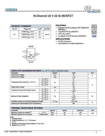
CES2320 Specs and Replacement
Type Designator: CES2320
Type of Transistor: MOSFET
Type of Control Channel: N-Channel
Absolute Maximum Ratings
Pd ⓘ - Maximum Power Dissipation: 1.3 W
|Vds|ⓘ - Maximum Drain-Source Voltage: 30 V
|Vgs|ⓘ - Maximum Gate-Source Voltage: 20 V
|Id| ⓘ - Maximum Drain Current: 5.2 A
Tj ⓘ - Maximum Junction Temperature: 150 °C
Electrical Characteristics
tr ⓘ - Rise Time: 5 nS
Cossⓘ - Output Capacitance: 130 pF
RDSonⓘ - Maximum Drain-Source On-State Resistance: 0.029 Ohm
Package: SOT23
CES2320 substitution
- MOSFET ⓘ Cross-Reference Search
CES2320 datasheet
ces2320.pdf

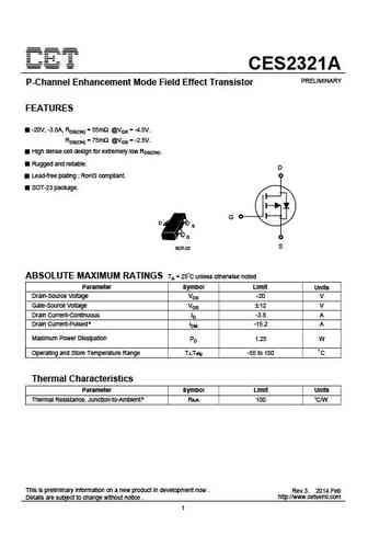
CES2320 N-Channel Enhancement Mode Field Effect Transistor FEATURES 30V, 5.2A, RDS(ON) = 29m @VGS = 10V. RDS(ON) = 45m @VGS = 4.5V. High dense cell design for extremely low RDS(ON). Lead free product is acquired. D Rugged and reliable. SOT-23 package. G D S G S SOT-23 ABSOLUTE MAXIMUM RATINGS TA = 25 C unless otherwise noted Parameter Symbol Limit Units Drain-Source Vol... See More ⇒
ces2322.pdf

CES2322 N-Channel Enhancement Mode Field Effect Transistor PRELIMINARY FEATURES 20V, 6.2A, RDS(ON) = 22m @VGS = 4.5V. RDS(ON) = 30m @VGS = 2.5V. High dense cell design for extremely low RDS(ON). Lead-free plating ; RoHS compliant. D Rugged and reliable. SOT-23 package. G D S G S SOT-23 ABSOLUTE MAXIMUM RATINGS TA = 25 C unless otherwise noted Parameter Symbol Limit Units... See More ⇒
ces2323.pdf

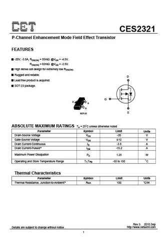
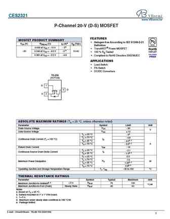
CES2323 P-Channel Enhancement Mode Field Effect Transistor FEATURES -30V, -4.2A, RDS(ON) = 48m @VGS = -10V. RDS(ON) = 80m @VGS = -4.5V. High dense cell design for extremely low RDS(ON). Rugged and reliable. D Lead free product is acquired. SOT-23 package. G D S G S SOT-23 ABSOLUTE MAXIMUM RATINGS TA = 25 C unless otherwise noted Parameter Symbol Limit Units Drain-Source... See More ⇒
ces2324.pdf

CES2324 N-Channel Enhancement Mode Field Effect Transistor FEATURES 20V, 4.2A, RDS(ON) = 45m @VGS = 4.5V. RDS(ON) = 80m @VGS = 2.5V. High dense cell design for extremely low RDS(ON). Lead free product is acquired. D Rugged and reliable. SOT-23 package. G D S G S SOT-23 ABSOLUTE MAXIMUM RATINGS TA = 25 C unless otherwise noted Parameter Symbol Limit Units Drain-Source Vo... See More ⇒
Detailed specifications: CEN7002A, CES2302, CES2306, CES2308, CES2310, CES2312, CES2314, CES2316, IRF1404, CES2324, CES2342, CES2362, CET0215, CET04N10, CET3055L, CET3252, CET6426
Keywords - CES2320 MOSFET specs
CES2320 cross reference
CES2320 equivalent finder
CES2320 pdf lookup
CES2320 substitution
CES2320 replacement
Step-by-step guide to finding a MOSFET replacement. Cross-reference parts and ensure compatibility for your repair or project.
🌐 : EN ES РУ

LIST
Last Update
MOSFET: AKF30N5P0SX | AKF30N10S | AKF20P45D | CM4407 | CM3407 | CM3400 | SVF11N65F | SVF11N65T | FKBB3105 | EHBA036R1
Popular searches
2sc869 datasheet | k3568 datasheet | 2sb77 | ac128 transistor datasheet | c2878 transistor | 2sc732 | 2sc1451 replacement | 6426 mosfet