CEB50P03 Specs and Replacement
Type Designator: CEB50P03
Type of Transistor: MOSFET
Type of Control Channel: P-Channel
Absolute Maximum Ratings
Pd ⓘ - Maximum Power Dissipation: 79 W
|Vds|ⓘ - Maximum Drain-Source Voltage: 30 V
|Vgs|ⓘ - Maximum Gate-Source Voltage: 20 V
|Id| ⓘ - Maximum Drain Current: 47 A
Tj ⓘ - Maximum Junction Temperature: 175 °C
Electrical Characteristics
tr ⓘ - Rise Time: 6 nS
Cossⓘ - Output Capacitance: 550 pF
RDSonⓘ - Maximum Drain-Source On-State Resistance: 0.02 Ohm
Package: TO263
CEB50P03 substitution
- MOSFET ⓘ Cross-Reference Search
CEB50P03 datasheet
cep50p03 ceb50p03.pdf
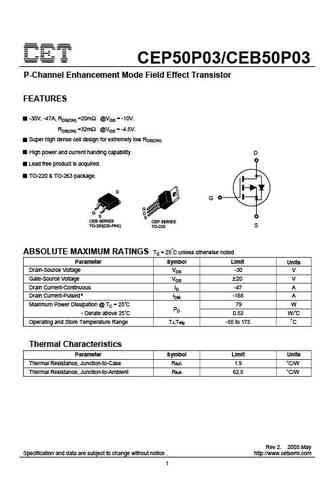
CEP50P03/CEB50P03 P-Channel Enhancement Mode Field Effect Transistor FEATURES -30V, -47A, RDS(ON) =20m @VGS = -10V. RDS(ON) =32m @VGS = -4.5V. Super high dense cell design for extremely low RDS(ON). High power and current handing capability. D Lead free product is acquired. TO-220 & TO-263 package. G CEB SERIES CEP SERIES TO-263(DD-PAK) S TO-220 ABSOLUTE MAXIMUM RATINGS Tc ... See More ⇒
ceb50p03.pdf
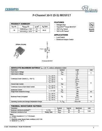
CEB50P03 www.VBsemi.tw P-Channel 30-V (D-S) MOSFET FEATURES PRODUCT SUMMARY Halogen-free VDS (V) RDS(on) ( ) ID (A)d Qg (Typ.) TrenchFET Power MOSFET 0.008 at VGS = - 10 V - 75 100 % Rg Tested RoHS - 30 56 nC COMPLIANT 100 % UIS Tested 0.011 at VGS = - 4.5 V - 65 APPLICATIONS Load Switch Notebook Adaptor Switch S D2PAK (TO-263) G D G S D P... See More ⇒
cep50n06 ceb50n06.pdf
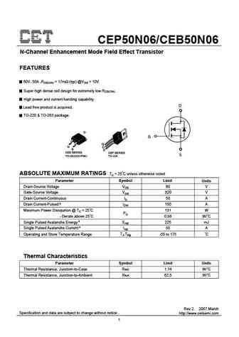
CEP50N06/CEB50N06 N-Channel Enhancement Mode Field Effect Transistor FEATURES 60V, 50A ,RDS(ON) = 17m (typ) @VGS = 10V. Super high dense cell design for extremely low RDS(ON). High power and current handing capability. D Lead free product is acquired. TO-220 & TO-263 package. G CEB SERIES CEP SERIES S TO-263(DD-PAK) TO-220 ABSOLUTE MAXIMUM RATINGS Tc = 25 C unless otherwise no... See More ⇒
cep50n10 ceb50n10.pdf
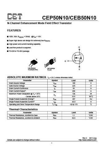
CEP50N10/CEB50N10 N-Channel Enhancement Mode Field Effect Transistor FEATURES 100V, 50A, RDS(ON) = 30m @VGS = 10V. Super high dense cell design for extremely low RDS(ON). High power and current handing capability. D Lead free product is acquired. TO-220 & TO-263 package. G CEB SERIES CEP SERIES S TO-263(DD-PAK) TO-220 ABSOLUTE MAXIMUM RATINGS Tc = 25 C unless otherwise noted ... See More ⇒
Detailed specifications: CEB05P03, CEB12P10, CEB14P20, CEB15P15, CEB20P06, CEB20P10, CEB30P03, CEB35P10, 2N7002, CEB6601, CEB95P04, CED05P03, CED11P20, CED12P10, CED20P06, CED20P10, CED2303
Keywords - CEB50P03 MOSFET specs
CEB50P03 cross reference
CEB50P03 equivalent finder
CEB50P03 pdf lookup
CEB50P03 substitution
CEB50P03 replacement
Learn how to find the right MOSFET substitute. A guide to cross-reference, check specs and replace MOSFETs in your circuits.
