FDN335N Specs and Replacement
Type Designator: FDN335N
Marking Code: 335
Type of Transistor: MOSFET
Type of Control Channel: N
-Channel
Absolute Maximum Ratings
Pd ⓘ
- Maximum Power Dissipation: 0.5
W
|Vds|ⓘ - Maximum Drain-Source Voltage: 20
V
|Vgs|ⓘ - Maximum Gate-Source Voltage: 8
V
|Id| ⓘ - Maximum Drain Current: 1.7
A
Tj ⓘ - Maximum Junction Temperature: 150
°C
Electrical Characteristics
|Vgs(th)|ⓘ - Maximum Gate-Threshold Voltage: 1.5
V
Qg ⓘ - Total Gate Charge: 3.5
nC
tr ⓘ - Rise Time: 8.5
nS
Cossⓘ -
Output Capacitance: 80
pF
Rds ⓘ - Maximum Drain-Source On-State Resistance: 0.07
Ohm
Package:
SUPERSOT3
-
MOSFET ⓘ Cross-Reference Search
FDN335N datasheet
..1. Size:81K fairchild semi
fdn335n.pdf 
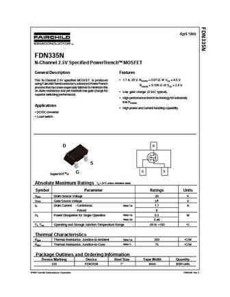
April 1999 FDN335N N-Channel 2.5V Specified PowerTrenchTM MOSFET General Description Features 1.7 A, 20 V. RDS(ON) = 0.07 @ VGS = 4.5 V This N-Channel 2.5V specified MOSFET is produced using Fairchild Semiconductor's advanced PowerTrench RDS(ON) = 0.100 @ VGS = 2.5 V. process that has been especially tailored to minimize the on-state resistance and yet maintain low gate cha... See More ⇒
..2. Size:198K onsemi
fdn335n.pdf
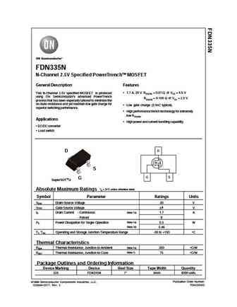
FDN335N N-Channel 2.5V Specified PowerTrenchTM MOSFET General Description Features 1.7 A, 20 V. RDS(ON) = 0.07 @ VGS = 4.5 V This N-Channel 2.5V specified MOSFET is produced using ON Semiconductor's advanced PowerTrench RDS(ON) = 0.100 @ VGS = 2.5 V. process that has been especially tailored to minimize the on-state resistance and yet maintain low gate charge for Lo... See More ⇒
..3. Size:1905K htsemi
fdn335n.pdf
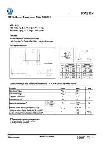
FDN335N 20V N-Channel Enhancement Mode MOSFET VDS= 20V RDS(ON), Vgs@ 2.5V, Ids@ 1.7A= 70m RDS(ON), Vgs@ 2.5V, Ids@ 1.5A= 100m Features Advanced trench process technology High Density Cell Design For Ultra Low On-Resistance Package Dimensions D G S SOT-23(PACKAGE) Millimeter Millimeter REF. REF. Min. Max. Min. Max. A 2.70 3.10 G 1.90 REF. B 2.40 2.80 H 1.00... See More ⇒
..4. Size:379K umw-ic
fdn335n.pdf
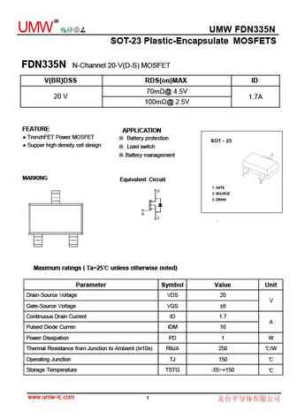
R UMW UMW FDN335N MOSFETS SOT-23 Plastic-Encapsulate FDN335N N-Channel 20-V(D-S) MOSFET V(BR)DSS RDS(on)MAX ID 70m @ 4.5V 20 V 1.7A 100m @ 2.5V FEATURE APPLICATION TrenchFET Power MOSFET Battery protection SOT 23 Supper high density cell design Load switch Battery management MARKING Equivalent Circuit 1. GATE 2. SOURCE 3. DRAIN Maximum ra... See More ⇒
..5. Size:422K huashuo
fdn335n.pdf
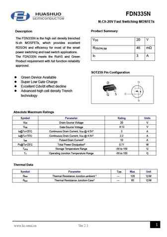
FDN335N N-Ch 20V Fast Switching MOSFETs Product Summary Description The FDN335N is the high cell density trenched V 20 V DS N-ch MOSFETs, which provides excellent RDSON and efficiency for most of the small R 46 m DS(ON),typ power switching and load switch applications. I 3 A D The FDN335N meets the RoHS and Green Product requirement with full function reliability ... See More ⇒
..6. Size:399K cn shikues
fdn335n.pdf
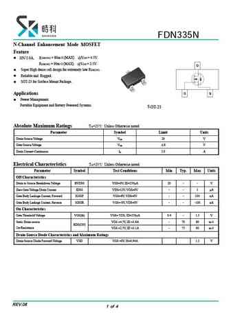
FDN335N N-Channel Enhancement Mode MOSFET Feature 20V/2.0A, RDS(ON) = 80m (MAX) @VGS = 4.5V. RDS(ON) = 90m (MAX) @VGS = 2.5V. Super High dense cell design for extremely low RDS(ON) . Reliable and Rugged. SOT-23 for Surface Mount Package. Applications Power Management Portable Equipment and Battery Powered Systems. S O T - 2 3 Absolute Maximum Ratings TA... See More ⇒
0.1. Size:1707K cn vbsemi
fdn335n-nl.pdf
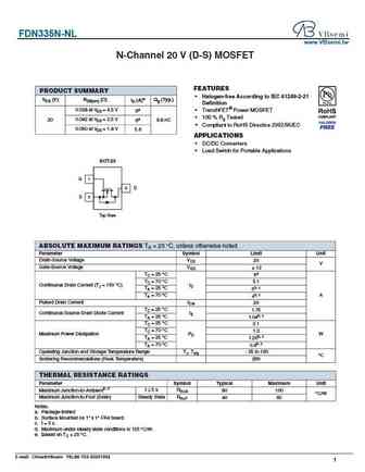
FDN335N-NL www.VBsemi.tw N-Channel 20 V (D-S) MOSFET FEATURES PRODUCT SUMMARY Halogen-free According to IEC 61249-2-21 VDS (V) RDS(on) ( ) ID (A)e Qg (Typ.) Definition 0.028 at VGS = 4.5 V TrenchFET Power MOSFET 6a 100 % Rg Tested 20 0.042 at VGS = 2.5 V 6a 8.8 nC Compliant to RoHS Directive 2002/95/EC 0.050 at VGS = 1.8 V 5.6 APPLICATIONS DC/D... See More ⇒
9.1. Size:73K fairchild semi
fdn336p-nl.pdf
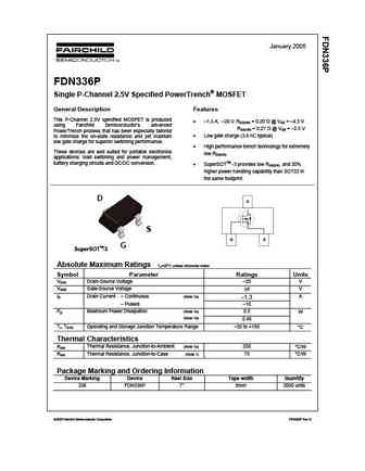
January 2005 FDN336P Single P-Channel 2.5V Specified PowerTrench MOSFET General Description Features This P-Channel 2.5V specified MOSFET is produced 1.3 A, 20 V. RDS(ON) = 0.20 @ VGS = 4.5 V using Fairchild Semiconductor s advanced RDS(ON) = 0.27 @ VGS = 2.5 V PowerTrench process that has been especially tailored Low gate charge (3.6 nC typical... See More ⇒
9.2. Size:276K fairchild semi
fdn337n.pdf
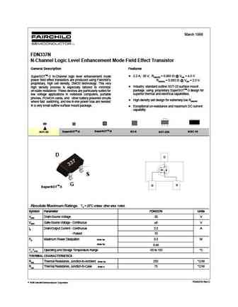
March 1998 FDN337N N-Channel Logic Level Enhancement Mode Field Effect Transistor General Description Features SuperSOTTM-3 N-Channel logic level enhancement mode 2.2 A, 30 V, RDS(ON) = 0.065 @ VGS = 4.5 V power field effect transistors are produced using Fairchild's RDS(ON) = 0.082 @ VGS = 2.5 V. proprietary, high cell density, DMOS technology. This very Industry standard... See More ⇒
9.3. Size:89K fairchild semi
fdn339an.pdf
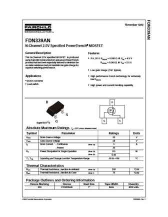
November 1999 FDN339AN N-Channel 2.5V Specified PowerTrench MOSFET General Description Features This N-Channel 2.5V specified MOSFET is produced 3 A, 20 V. RDS(ON) = 0.035 @ VGS = 4.5 V using Fairchild Semiconductor's advanced PowerTrench process that has been especially tailored to minimize the RDS(ON) = 0.050 @ VGS = 2.5 V. on-state resistance and y... See More ⇒
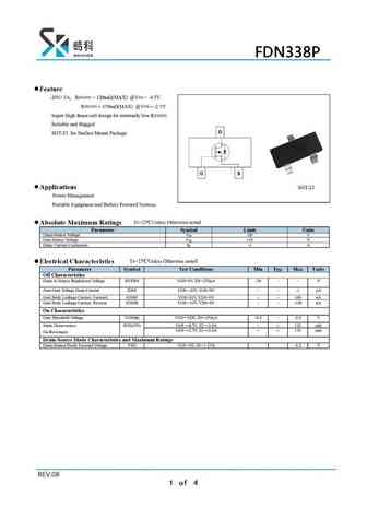
9.4. Size:267K fairchild semi
fdn338p.pdf
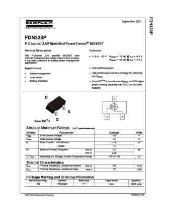
September 2001 FDN338P P-Channel 2.5V Specified PowerTrench MOSFET General Description Features This P-Channel 2.5V specified MOSFET uses 1.6 A, 20 V. R = 115 m @ V = 4.5 V DS(ON) GS Fairchild s advanced low voltage PowerTrench process. R = 155 m @ V = 2.5 V DS(ON) GS It has been optimized for battery power management applications. Fast switchi... See More ⇒
9.5. Size:391K onsemi
fdn337n.pdf

Is Now Part of To learn more about ON Semiconductor, please visit our website at www.onsemi.com Please note As part of the Fairchild Semiconductor integration, some of the Fairchild orderable part numbers will need to change in order to meet ON Semiconductor s system requirements. Since the ON Semiconductor product management systems do not have the ability to manage part nomenclatur... See More ⇒
9.6. Size:66K onsemi
fdn336p.pdf
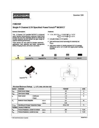
November 1998 FDN336P Single P-Channel 2.5V Specified PowerTrenchTM MOSFET General Description Features This P-Channel 2.5V specified MOSFET is produced -1.3 A, -20 V. RDS(ON) = 0.20 @ VGS = -4.5 V using Fairchild Semiconductor's advanced PowerTrench RDS(ON) = 0.27 @ VGS= -2.5 V. process that has been especially tailored to minimize the Low gate charge (3.6 nC typical).... See More ⇒
9.7. Size:321K onsemi
fdn338p.pdf
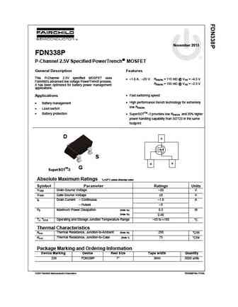
November 2013 FDN338P P-Channel 2.5V Specified PowerTrench MOSFET General Description Features This P-Channel 2.5V specified MOSFET uses 1.6 A, 20 V. R = 115 m @ V = 4.5 V DS(ON) GS Fairchild s advanced low voltage PowerTrench process. R = 155 m @ V = 2.5 V DS(ON) GS It has been optimized for battery power management applications. Fast switching... See More ⇒
9.8. Size:1909K htsemi
fdn338p.pdf
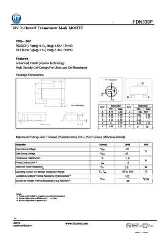
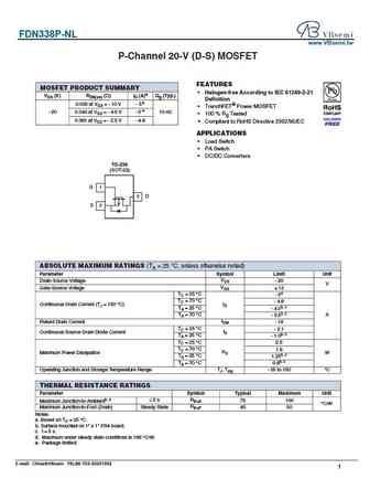
FDN338P 20V P-Channel Enhancement Mode MOSFET VDS= -20V 115m RDS(ON), Vgs@-4.5V, Ids@-1.6A= RDS(ON), Vgs@-2.5V, Ids@-1.3A= 155m Features Advanced trench process technology High Density Cell Design For Ultra Low On-Resistance Package Dimensions D G S SOT-23(PACKAGE) Millimeter Millimeter REF. REF. Min. Max. Min. Max. A 2.70 3.10 G 1.90 REF. B 2.40 2.80 H 1.... See More ⇒
9.9. Size:1818K shenzhen
fdn338.pdf
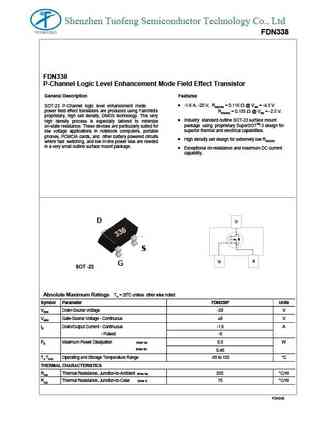
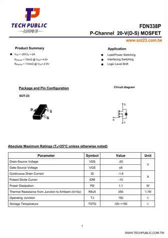
Shenzhen Tuofeng Semiconductor Technology Co., Ltd FDN338 FDN338 P-Channel Logic Level Enhancement Mode Field Effect Transistor General Description Features SOT-23 P-Channel logic level enhancement mode -1.6 A, -20 V, RDS(ON) = 0.115 @ VGS = -4.5 V power field effect transistors are produced using Fairchild's RDS(ON) = 0.155 @ VGS = -2.5 V. proprietary, high cell density, ... See More ⇒
9.10. Size:98K kexin
fdn336p.pdf
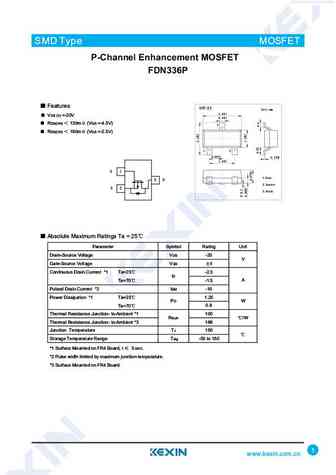
SMD Type MOSFET P-Channel Enhancement MOSFET FDN336P Features SOT-23 Unit mm 2.9+0.1 -0.1 VDS (V) =-20V +0.1 0.4 -0.1 RDS(ON) 130m (VGS =-4.5V) 3 RDS(ON) 190m (VGS =-2.5V) 12 +0.1 +0.05 0.95-0.1 0.1 -0.01 1.9+0.1 -0.1 G 1 1.Gate 3 D 2.Source S 2 3.Drain Absolute Maximum Ratings Ta = 25 Parameter Symbol Rating Unit Drain-Source Voltage VDS -20 V Gate-Source... See More ⇒
9.11. Size:596K umw-ic
fdn338p.pdf
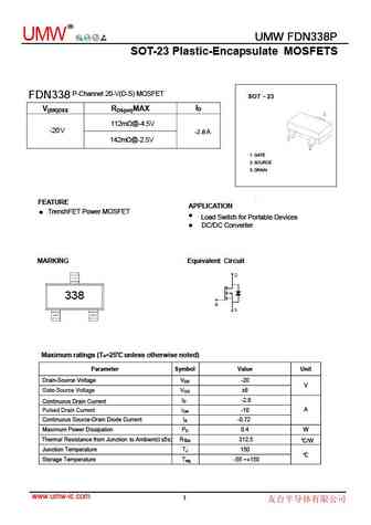
R UMW UMW FDN338P UMW FDN338P SOT-23 Plastic-Encapsulate MOSFETS P-Channel 20-V(D-S) MOSFET FDN338 SOT 23 ID V(BR)DSS RDS(on)MAX 112m @-4.5V -20V A -2.8 142m @-2.5V 1. GATE 2. SOURCE 3. DRAIN FEATURE APPLICATION TrenchFET Power MOSFET z z Load Switch for Portable Devices z DC/DC Converter MARKING Equivalent Circuit 338 Maximum ratings (Ta=25 u... See More ⇒
9.12. Size:498K huashuo
fdn338p.pdf
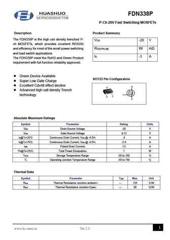
FDN338P P-Ch 20V Fast Switching MOSFETs Description Product Summary The FDN338P is the high cell density trenched P- VDS -20 V ch MOSFETs, which provides excellent RDSON and efficiency for most of the small power switching RDS(ON),typ 89 m and load switch applications. ID -3 A The FDN338P meet the RoHS and Green Product requirement with full function reliability approved. ... See More ⇒
9.13. Size:399K cn shikues
fdn337n.pdf
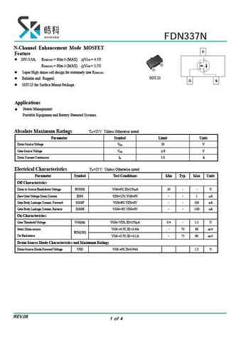
FDN337N N-Channel Enhancement Mode MOSFET Feature 20V/3.0A, RDS(ON) = 80m (MAX) @VGS = 4.5V. RDS(ON) = 90m (MAX) @VGS = 2.5V. Super High dense cell design for extremely low RDS(ON) . SOT-23 Reliable and Rugged. SOT-23 for Surface Mount Package. Applications Power Management Portable Equipment and Battery Powered Systems. Absolute Maximum Ratings TA=25 Unl... See More ⇒
9.14. Size:1031K cn shikues
fdn336p.pdf
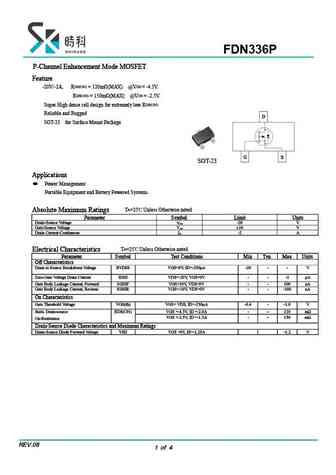
FDN336P P-Channel Enhancement Mode MOSFET Feature -20V/-2A, RDS(ON) = 120m (MAX) @VGS = -4.5V. DS(ON) GS R = 150m (MAX) @V = -2.5V. DS(ON) Super High dense cell design for extremely low R Reliable and Rugged SOT-23 for Surface Mount Package SOT-23 Applications Power Management Portable Equipment and Battery Powered Systems. A T =25 Unless Otherwise noted Ab... See More ⇒
9.16. Size:869K cn vbsemi
fdn338p-nl.pdf
FDN338P-NL www.VBsemi.tw P-Channel 20-V (D-S) MOSFET FEATURES MOSFET PRODUCT SUMMARY Halogen-free According to IEC 61249-2-21 VDS (V) RDS(on) ( )ID (A)a Qg (Typ.) Definition 0.035 at VGS = - 10 V - 5e TrenchFET Power MOSFET e - 20 0.043 at VGS = - 4.5 V - 5 10 nC 100 % Rg Tested 0.061 at VGS = - 2.5 V - 4.8 Compliant to RoHS Directive 2002/95/EC APPLICATI... See More ⇒
9.17. Size:1722K cn vbsemi
fdn337n-nl.pdf
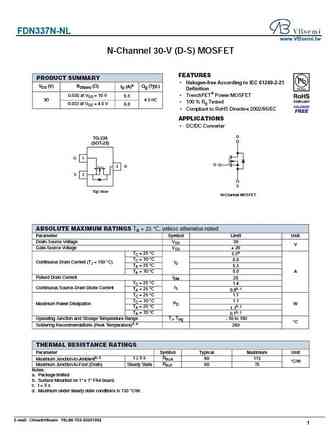
FDN337N-NL www.VBsemi.tw N-Channel 30-V (D-S) MOSFET FEATURES PRODUCT SUMMARY Halogen-free According to IEC 61249-2-21 VDS (V) RDS(on) ( ) ID (A)a Qg (Typ.) Definition 0.030 at VGS = 10 V TrenchFET Power MOSFET 6.5 30 4.5 nC 100 % Rg Tested 0.033 at VGS = 4.5 V 6.0 Compliant to RoHS Directive 2002/95/EC APPLICATIONS DC/DC Converter D TO-236 (SOT-23) ... See More ⇒
Detailed specifications: FDG313N
, FDG314P
, FDG315N
, FDG316P
, FDG6301N
, FDG6302P
, FDG6303N
, FDG6304P
, IRF830
, FDN336P
, FDN337N
, FDN338P
, FDN339AN
, FDN340P
, FDN357N
, FDN358P
, FDN359AN
.
Keywords - FDN335N MOSFET specs
FDN335N cross reference
FDN335N equivalent finder
FDN335N pdf lookup
FDN335N substitution
FDN335N replacement
Need a MOSFET replacement?
Our guide shows you how to find a perfect substitute by comparing key parameters and specs