PN4119A Datasheet. Specs and Replacement
Type Designator: PN4119A 📄📄
Type of Transistor: JFET
Type of Control Channel: N-Channel
Absolute Maximum Ratings
Pd ⓘ - Maximum Power Dissipation: 0.3 W
|Vds|ⓘ - Maximum Drain-Source Voltage: 40 V
|Vgs|ⓘ - Maximum Gate-Source Voltage: 6 V
|Id| ⓘ - Maximum Drain Current: 0.05 A
Tj ⓘ - Maximum Junction Temperature: 135 °C
Electrical Characteristics
Package: TO-92
📄📄 Copy
PN4119A substitution
- MOSFET ⓘ Cross-Reference Search
PN4119A datasheet
2n4117a pn4117a sst4117 2n4118a pn4118a sst4118 2n4119a pn4119a sst4119.pdf
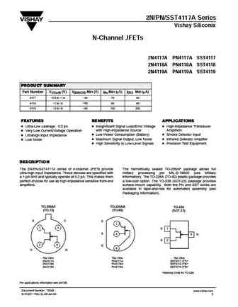
2N/PN/SST4117A Series Vishay Siliconix N-Channel JFETs 2N4117A PN4117A SST4117 2N4118A PN4118A SST4118 2N4119A PN4119A SST4119 PRODUCT SUMMARY Part Number VGS(off) (V) V(BR)GSS Min (V) gfs Min (mS) IDSS Min (mA) 4117 -0.6 to -1.8 -40 70 30 4118 -1 to -3 -40 80 80 4119 -2 to -6 -40 100 200 FEATURES BENEFITS APPLICATIONS D Ultra-Low Leakage 0.2 pA D Insignificant Signal Loss/Error Vo... See More ⇒
pn4117 pn4118 pn4119 mmbf4117 mmbf4118 mmbf4119.pdf

PN4117 MMBF4117 PN4118 MMBF4118 PN4119 MMBF4119 G S G TO-92 S SOT-23 D D Mark 61A / 61C / 61E NOTE Source & Drain are interchangeable N-Channel Switch This device is designed for low current DC and audio applications. These devices provide excellent performance as input stages for sub-picoamp instrumentation or any high impedance signal sources. Sourced from Process 53. Abso... See More ⇒
2n4117 2n4118 2n4119 pn4117 pn4118 pn4119 sst4117 sst4118 sst4119.pdf
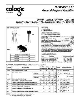
N-Channel JFET General Purpose Amplifier CORPORATION 2N4117 2N4119 / 2N4117A 2N4119A PN4117 PN4119 / PN4117A PN4119A / SST4117 SST4119 FEATURES PIN CONFIGURATION Low Leakage Low Capacitance ABSOLUTE MAXIMUM RATINGS TO-92 (T = 25oC unless otherwise noted) A TO-72 Gate-Source or Gate-Drain Voltage . . . . . . . . . . . . . . . . -40V Gate Curre... See More ⇒
pn4117a.pdf
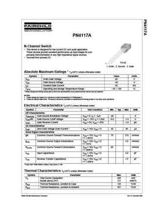
PN4117A N-Channel Switch This device is designed for low current DC and audio application. These devices provide excellent performance as input stages for sub- picoamp instrumentation or any high impedance signal sources. Sourced from process 53. TO-92 1 1. Drain 2. Source 3. Gate Absolute Maximum Ratings * TA=25 C unless otherwise noted Symbol Parameter Value Units VDG Dra... See More ⇒
Detailed specifications: 2N4117A, 2N4118A, 2N4119A, PN4117, PN4118, PN4119, PN4117A, PN4118A, K3569, SST4117, SST4118, SST4119, 2N4220, 2N4221, 2N4222, 2N4220A, 2N4221A
Keywords - PN4119A MOSFET specs
PN4119A cross reference
PN4119A equivalent finder
PN4119A pdf lookup
PN4119A substitution
PN4119A replacement
Can't find your MOSFET? Learn how to find a substitute transistor by analyzing voltage, current and package compatibility
MOSFET Parameters. How They Affect Each Other
🌐 : EN ES РУ

LIST
Last Update
MOSFET: MSQ60P04D | MSQ40P07D | MSQ30P40D | MSQ30P15 | MSQ30P07D | MSQ100N03D | MSHM60P14 | MSHM40N085 | MSHM30N46 | MSH60N35D
Popular searches
2sb1243 | a1123 transistor | skd502t datasheet | svf7n65f | 2sc1419 datasheet | 2n4249 datasheet | tip130 | se9302 transistor