J175 Specs and Replacement
Type Designator: J175
Type of Transistor: JFET
Type of Control Channel: P-Channel
Absolute Maximum Ratings
Pd ⓘ
- Maximum Power Dissipation: 0.35 W
|Vds|ⓘ - Maximum Drain-Source Voltage: 30 V
|Vgs|ⓘ - Maximum Gate-Source Voltage: 6 V
|Id| ⓘ - Maximum Drain Current: 0.06 A
Tj ⓘ - Maximum Junction Temperature: 150 °C
Electrical Characteristics
RDSonⓘ - Maximum Drain-Source On-State Resistance: 125 Ohm
Package: TO-92
- MOSFET ⓘ Cross-Reference Search
J175 datasheet
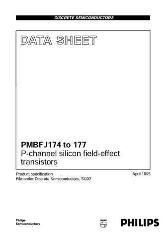
..1. Size:30K philips
j174 j175 j176 j177 cnv 2.pdf 

DISCRETE SEMICONDUCTORS DATA SHEET J174; J175; J176; J177 P-channel silicon field-effect transistors April 1995 Product specification File under Discrete Semiconductors, SC07 Philips Semiconductors Product specification J174; J175; P-channel silicon field-effect transistors J176; J177 DESCRIPTION Silicon symmetrical p-channel junction FETs in a plastic TO-92 envelope and intend... See More ⇒
..2. Size:728K fairchild semi
j174 j175 j176 j177 mmbfj175 mmbfj176 mmbfj177.pdf 

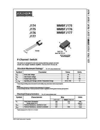
J174 MMBFJ175 J175 MMBFJ176 J176 MMBFJ177 J177 G S S TO-92 D SOT-23 G D Mark 6W / 6X / 6Y NOTE Source & Drain are interchangeable P-Channel Switch This device is designed for low level analog switching sample and hold circuits and chopper stabilized amplifiers. Sourced from Process 88. Absolute Maximum Ratings* TA = 25 C unless otherwise noted Symbol Parameter Value Units ... See More ⇒
..3. Size:56K vishay
j174 j175 j176 j177 sst174 sst175 sst176 sst177.pdf 

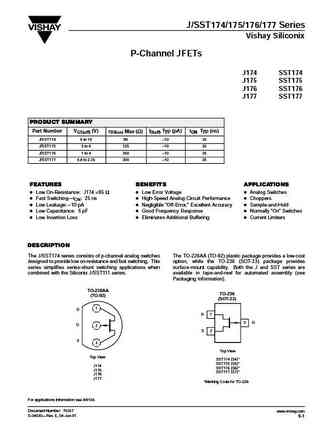
J/SST174/175/176/177 Series Vishay Siliconix P-Channel JFETs J174 SST174 J175 SST175 J176 SST176 J177 SST177 PRODUCT SUMMARY Part Number VGS(off) (V) rDS(on) Max (W) ID(off) Typ (pA) tON Typ (ns) J/SST174 5 to 10 85 10 25 J/SST175 3 to 6 125 10 25 J/SST176 1 to 4 250 10 25 J/SST177 0.8 to 2.25 300 10 25 FEATURES BENEFITS APPLICATIONS D Low On-Resistance J174 ... See More ⇒
0.1. Size:76K motorola
mmbfj175.pdf 

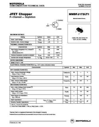
MOTOROLA Order this document SEMICONDUCTOR TECHNICAL DATA by MMBFJ175LT1/D JFET Chopper MMBFJ175LT1 P Channel Depletion Motorola Preferred Device 2 SOURCE 3 GATE 3 1 DRAIN 1 2 MAXIMUM RATINGS Rating Symbol Value Unit CASE 318 08, STYLE 10 SOT 23 (TO 236AB) Drain Gate Voltage VDG 25 V Reverse Gate Source Voltage VGS(r) 25 V THERMAL CHARACTERISTICS Charact... See More ⇒
0.2. Size:56K motorola
mmbfj175lt1rev0d.pdf 

MOTOROLA Order this document SEMICONDUCTOR TECHNICAL DATA by MMBFJ175LT1/D JFET Chopper MMBFJ175LT1 P Channel Depletion Motorola Preferred Device 2 SOURCE 3 GATE 3 1 DRAIN 1 2 MAXIMUM RATINGS Rating Symbol Value Unit CASE 318 08, STYLE 10 SOT 23 (TO 236AB) Drain Gate Voltage VDG 25 V Reverse Gate Source Voltage VGS(r) 25 V THERMAL CHARACTERISTICS Charact... See More ⇒
0.3. Size:31K philips
pmbfj174 pmbfj175 pmbfj176 pmbfj177 cnv 2.pdf 

DISCRETE SEMICONDUCTORS DATA SHEET PMBFJ174 to 177 P-channel silicon field-effect transistors April 1995 Product specification File under Discrete Semiconductors, SC07 Philips Semiconductors Product specification P-channel silicon field-effect transistors PMBFJ174 to 177 DESCRIPTION Silicon symmetrical p-channel junction FETs in plastic microminiature SOT23 envelopes.They are int... See More ⇒
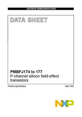
0.4. Size:57K nxp
pmbfj174 pmbfj175 pmbfj176 pmbfj177.pdf 

DISCRETE SEMICONDUCTORS DATA SHEET PMBFJ174 to 177 P-channel silicon field-effect transistors Product specification April 1995 NXP Semiconductors Product specification P-channel silicon field-effect transistors PMBFJ174 to 177 DESCRIPTION Silicon symmetrical p-channel junction FETs in plastic microminiature SOT23 envelopes.They are intended for application with analogue swi... See More ⇒
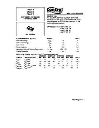
0.5. Size:202K central
cmpfj175 cmpfj176.pdf 

CMPFJ174 CMPFJ175 CMPFJ176 www.centralsemi.com CMPFJ177 DESCRIPTION SURFACE MOUNT SILICON The CENTRAL SEMICONDUCTOR CMPFJ174 P-CHANNEL JFETS Series devices are epoxy molded P-Channel JFETs manufactured in an SOT-23 case, designed for low level amplifier applications. MARKING CODES CMPFJ174 6V CMPFJ175 6W CMPFJ176 6X CMPFJ177 6Y SOT-23 CASE MAXIMUM RATINGS (TA=25 C)... See More ⇒
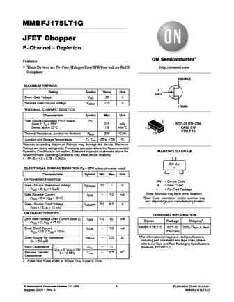
0.6. Size:105K onsemi
mmbfj175lt1.pdf 

MMBFJ175LT1G JFET Chopper P-Channel - Depletion Features These Devices are Pb-Free, Halogen Free/BFR Free and are RoHS http //onsemi.com Compliant 2 SOURCE MAXIMUM RATINGS 3 Rating Symbol Value Unit GATE Drain-Gate Voltage VDG 25 V Reverse Gate-Source Voltage VGS(r) -25 V 1 DRAIN THERMAL CHARACTERISTICS Characteristic Symbol Max Unit Total Device Dissipation FR-5 Board, PD ... See More ⇒
0.7. Size:29K hitachi
2sj175.pdf 

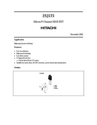
2SJ175 Silicon P-Channel MOS FET November 1996 Application High speed power switching Features Low on-resistance High speed switching Low drive current 4 V gate drive device Can be driven from 5 V source Suitable for motor drive, DC-DC converter, power switch and solenoid drive Outline TO-220FM D 1 2 3 1. Gate G 2. Drain 3. Source S 2SJ175 Abso... See More ⇒
0.8. Size:23K semelab
sml20j175.pdf 

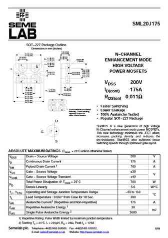
SML20J175 SOT 227 Package Outline. Dimensions in mm (inches) 11.8 (0.463) 12.2 (0.480) 31.5 (1.240) N CHANNEL 31.7 (1.248) 8.9 (0.350) 7.8 (0.307) 4.1 (0.161 ) 8.2 (0.322) W = 9.6 (0.378) Hex Nut M 4 4.3 (0.169 ) ENHANCEMENT MODE (4 places) 4.8 (0.187) H = 4.9 (0.193) 1 2 (4 places) HIGH VOLTAGE R POWER MOSFETS 4.0 (0.157) 0.75 (0.030) 4.2 (0.165) 0.85 (0.033) 4 3 ... See More ⇒
0.9. Size:181K semelab
sml20j175f.pdf 

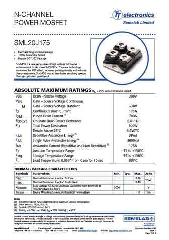
N-CHANNEL POWER MOSFET SML20J175 Fast Switching and Low leakage 100% Avalanche Tested Popular SOT-227 Package StarMOS is a new generation of high voltage N-Channel enhancement mode power MOSFET s. This new technology minimises the JFET effect, increases packing density and reduces the on-resistance. StarMOS also achieve faster switching speeds through optimised... See More ⇒
Detailed specifications: ISL9N303AP3
, ISL9N303AS3ST
, ISL9N303AS3
, J105
, J106
, J107
, JFTJ105
, J174
, 60N06
, J176
, J177
, MMBFJ175
, MMBFJ176
, MMBFJ177
, J201
, J202
, MMBFJ201
.
Keywords - J175 MOSFET specs
J175 cross reference
J175 equivalent finder
J175 pdf lookup
J175 substitution
J175 replacement
Learn how to find the right MOSFET substitute. A guide to cross-reference, check specs and replace MOSFETs in your circuits.
