MMBFJ310 Specs and Replacement
Type Designator: MMBFJ310
Type of Transistor: JFET
Type of Control Channel: N-Channel
Absolute Maximum Ratings
Pd ⓘ - Maximum Power Dissipation: 0.35 W
|Vds|ⓘ - Maximum Drain-Source Voltage: 25 V
|Vgs|ⓘ - Maximum Gate-Source Voltage: 6.5 V
|Id| ⓘ - Maximum Drain Current: 0.06 A
Tj ⓘ - Maximum Junction Temperature: 150 °C
Electrical Characteristics
Package: SOT-23
MMBFJ310 substitution
- MOSFET ⓘ Cross-Reference Search
MMBFJ310 datasheet
mmbfj309 mmbfj310.pdf
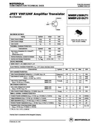
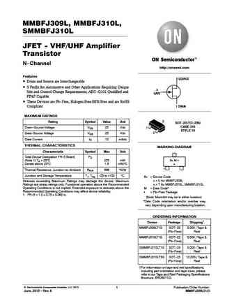
MOTOROLA Order this document SEMICONDUCTOR TECHNICAL DATA by MMBFJ309LT1/D JFET VHF/UHF Amplifier Transistor MMBFJ309LT1 N Channel 2 SOURCE MMBFJ310LT1 3 GATE 1 DRAIN 3 1 MAXIMUM RATINGS 2 Rating Symbol Value Unit Drain Source Voltage VDS 25 Vdc CASE 318 08, STYLE 10 Gate Source Voltage VGS 25 Vdc SOT 23 (TO 236AB) Gate Current IG 10 mAdc THERMAL CHARACTERISTICS... See More ⇒
j309 j310 mmbfj309 mmbfj310.pdf
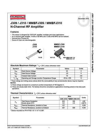
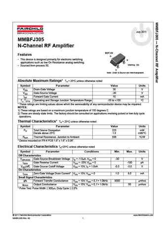
December 2010 J309 / J310 / MMBFJ309 / MMBFJ310 N-Channel RF Amplifier Features This device is designed for VHF/UHF amplifier, oscillator and mixer applications. As a common gate amplifier, 16 dB at 100 MHz and 12 dB at 450 MHz can be realized. Sourced from Process 92. Source & Drain are interchangeable. J309 MMBFJ309 J310 MMBFJ310 G S SOT-23 G TO-92 Mark MMBFJ309 ... See More ⇒
mmbfj310.pdf
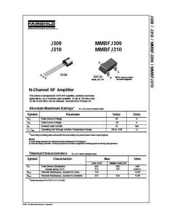
J309 MMBFJ309 J310 MMBFJ310 G S G TO-92 S SOT-23 NOTE Source & Drain D D are interchangeable Mark 6U / 6T N-Channel RF Amplifier This device is designed for VHF/UHF amplifier, oscillator and mixer applications. As a common gate amplifier, 16 dB at 100 MHz and 12 dB at 450 MHz can be realized. Sourced from Process 92. Absolute Maximum Ratings* TA = 25 C unless otherwise noted ... See More ⇒
mmbfj309lt1 mmbfj310lt1.pdf
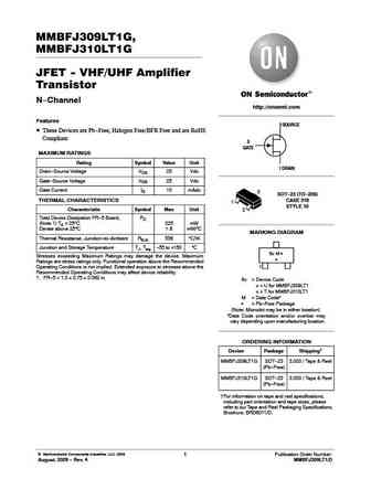
MMBFJ309LT1G, MMBFJ310LT1G JFET - VHF/UHF Amplifier Transistor N-Channel http //onsemi.com Features 2 SOURCE These Devices are Pb-Free, Halogen Free/BFR Free and are RoHS Compliant 3 GATE MAXIMUM RATINGS Rating Symbol Value Unit 1 DRAIN Drain-Source Voltage VDS 25 Vdc Gate-Source Voltage VGS 25 Vdc Gate Current IG 10 mAdc 3 SOT-23 (TO-236) THERMAL CHARACTERISTICS CASE 31... See More ⇒
Detailed specifications: MMBF5462 , MMBF5484 , MMBF5485 , MMBF5486 , MMBFJ270 , MMBFJ271 , J309 , MMBFJ309 , AON6380 , MPF102 , P1086 , P1087 , STP11NB40 , STP11NB40FP , STP9NB50 , STP9NB50FP , PF5102 .
Keywords - MMBFJ310 MOSFET specs
MMBFJ310 cross reference
MMBFJ310 equivalent finder
MMBFJ310 pdf lookup
MMBFJ310 substitution
MMBFJ310 replacement
Need a MOSFET replacement? Our guide shows you how to find a perfect substitute by comparing key parameters and specs
🌐 : EN ES РУ
LIST
Last Update
MOSFET: ASB80R750E | ASB70R380E | ASB65R300E | ASB65R220E | ASB65R120EFD | ASB60R150E | ASA80R900E | ASA80R750E | ASA80R290E | ASA70R950E
Popular searches
irf3710 | tip3055 | mosfet datasheet | irf3205 datasheet | irf5210 | mj15024 | 2n2219 | tip42c
