3N80 Specs and Replacement
Type Designator: 3N80
Type of Transistor: MOSFET
Type of Control Channel: N-Channel
Absolute Maximum Ratings
Pd ⓘ - Maximum Power Dissipation: 70 W
|Vds|ⓘ - Maximum Drain-Source Voltage: 800 V
|Vgs|ⓘ - Maximum Gate-Source Voltage: 30 V
|Id| ⓘ - Maximum Drain Current: 3 A
Tj ⓘ - Maximum Junction Temperature: 150 °C
Electrical Characteristics
tr ⓘ - Rise Time: 27 nS
Cossⓘ - Output Capacitance: 57 pF
RDSonⓘ - Maximum Drain-Source On-State Resistance: 3.2 Ohm
Package: TO-220 TO-251 TO-252 TO-220F TO-220F1
3N80 substitution
- MOSFET ⓘ Cross-Reference Search
3N80 datasheet
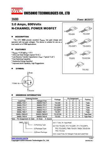
3n80.pdf
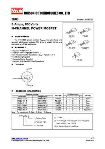
UNISONIC TECHNOLOGIES CO., LTD 3N80 Power MOSFET 3 Amps, 800Volts N-CHANNEL POWER MOSFET DESCRIPTION The UTC 3N80 provide excellent RDS(ON), low gate charge and operation with low gate voltages. This device is suitable for use as a load switch or in PWM applications. FEATURES * RDS(ON)=3.2 @VGS=10 V * Ultra Low Gate Charge ( typical 19 nC ) * Low Reverse Transfer... See More ⇒
3n80.pdf
isc N-Channel MOSFET Transistor 3N80 FEATURES Drain Current I =3.0A@ T =25 D C Drain Source Voltage- V = 800V(Min) DSS Static Drain-Source On-Resistance R = 4.5 (Max) DS(on) Fast Switching Minimum Lot-to-Lot variations for robust device performance and reliable operation APPLICATIONS Switching power supplies,converters,AC and DC motor controls ABSOLUTE M... See More ⇒
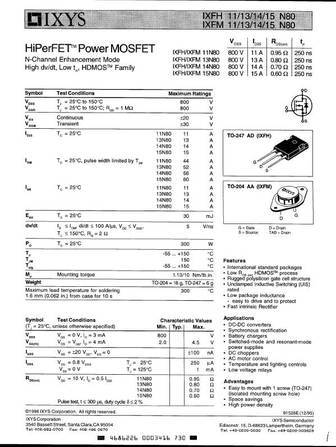
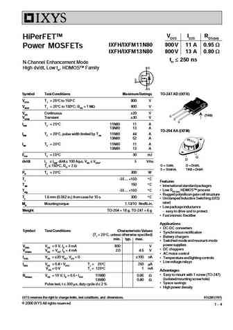
ixfh11n80 ixfm11n80 ixfh13n80 ixfm13n80 ixfh14n80 ixfm14n80 ixfh15n80 ixfm15n80.pdf
... See More ⇒
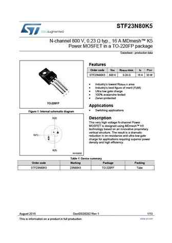
stf23n80k5.pdf
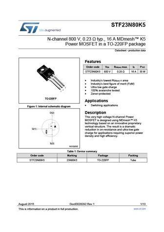
STF23N80K5 N-channel 800 V, 0.23 typ., 16 A MDmesh K5 Power MOSFET in a TO-220FP package Datasheet - production data Features Order code V R max. I P DS DS(on) D TOT STF23N80K5 800 V 0.28 16 A 35 W Industry s lowest R x area DS(on) Industry s best figure of merit (FoM) Ultra low gate charge 100% avalanche tested Zener-protected TO-220F... See More ⇒
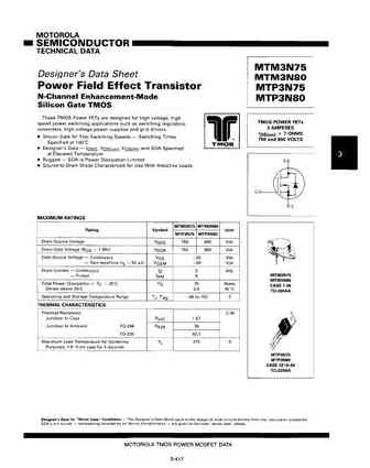
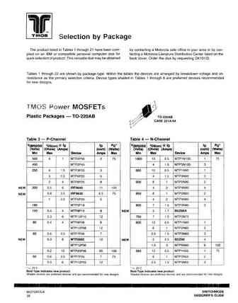
mtp1n100 mtp1n55 mtp1n95 mtp20p06 mtp2955 mtp2n55 mtp2n60 mtp2n85 mtp2p45 mtp2p50 mtp3n100 mtp3n75 mtp3n80 mtp3n95 mtp3p25 mtp4n85.pdf
... See More ⇒
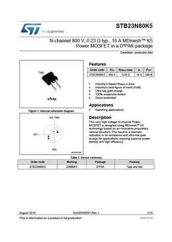
stb23n80k5.pdf
STB23N80K5 N-channel 800 V, 0.23 typ., 16 A MDmesh K5 Power MOSFET in a D PAK package Datasheet - production data Features Order code V R max. I P DS DS(on) D TOT TAB STB23N80K5 800 V 0.28 16 A 190 W Industry s lowest R x area DS(on) 3 Industry s best figure of merit (FoM) 1 Ultra low gate charge 100% avalanche tested Zener-protected... See More ⇒
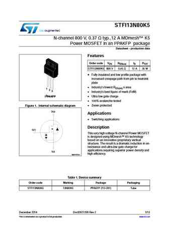
stfi13n80k5.pdf
STFI13N80K5 N-channel 800 V, 0.37 typ.,12 A MDmesh K5 Power MOSFET in an I PAKFP package Datasheet - production data Features Order code VDS RDS(on) ID PTOT STFI13N80K5 800 V 0.45 12 A 35 W Fully insulated and low profile package with increased creepage path from pin to heatsink plate Industry s lowest RDS(on) x area 1 2 3 Industry s best figure of ... See More ⇒
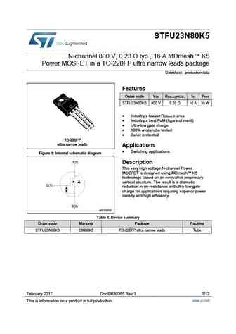
stfu23n80k5.pdf
STFU23N80K5 N-channel 800 V, 0.23 typ., 16 A MDmesh K5 Power MOSFET in a TO-220FP ultra narrow leads package Datasheet - production data Features Order code V R max. I P DS DS(on) D TOT STFU23N80K5 800 V 0.28 16 A 35 W Industry s lowest R x area DS(on) Industry s best FoM (figure of merit) Ultra-low gate charge 3 2 1 100% avalanche tested ... See More ⇒
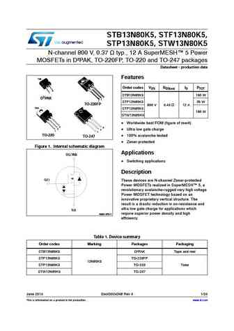
stb13n80k5 stf13n80k5 stp13n80k5 stw13n80k5.pdf
STB13N80K5, STF13N80K5, STP13N80K5, STW13N80K5 N-channel 800 V, 0.37 typ., 12 A SuperMESH 5 Power MOSFETs in D PAK, TO-220FP, TO-220 and TO-247 packages Datasheet - production data Features TAB Order codes VDS RDS(on) ID PTOT 3 1 STB13N80K5 190 W 3 D2PAK 2 1 STF13N80K5 35 W TO-220FP 800 V 0.45 12 A TAB STP13N80K5 190 W STW13N80K5 Worldwide best FOM (figur... See More ⇒
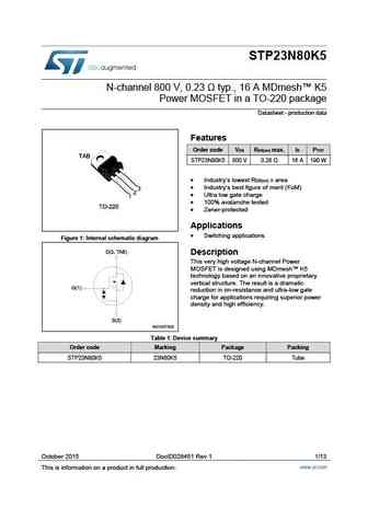
stp23n80k5.pdf
STP23N80K5 N-channel 800 V, 0.23 typ., 16 A MDmesh K5 Power MOSFET in a TO-220 package Datasheet - production data Features Order code V R max. I P DS DS(on) D TOT STP23N80K5 800 V 0.28 16 A 190 W Industry s lowest R x area DS(on) Industry s best figure of merit (FoM) Ultra low gate charge 100% avalanche tested Zener-protected Applicat... See More ⇒
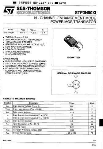
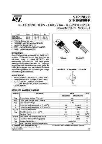
stp3n80.pdf
STP3NB80 STP3NB80FP N - CHANNEL 800V - 4.6 - 2.6A - TO-220/TO-220FP PowerMESH MOSFET TYPE VDSS RDS(on) ID STP3NB80 800 V ... See More ⇒
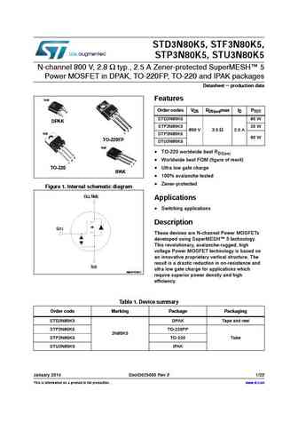
std3n80k5 stf3n80k5 stp3n80k5 stu3n80k5.pdf
STD3N80K5, STF3N80K5, STP3N80K5, STU3N80K5 N-channel 800 V, 2.8 typ., 2.5 A Zener-protected SuperMESH 5 Power MOSFET in DPAK, TO-220FP, TO-220 and IPAK packages Datasheet - production data Features TAB Order codes VDS RDS(on)max ID PTOT 3 1 STD3N80K5 60 W DPAK STF3N80K5 20 W 3 800 V 3.5 2.5 A 2 1 TAB STP3N80K5 60 W TO-220FP STU3N80K5 TAB TO-220 worldwide bes... See More ⇒
stf23n80k5.pdf
STF23N80K5 N-channel 800 V, 0.23 typ., 16 A MDmesh K5 Power MOSFET in a TO-220FP package Datasheet - production data Features Order code V R max. I P DS DS(on) D TOT STF23N80K5 800 V 0.28 16 A 35 W Industry s lowest R x area DS(on) Industry s best figure of merit (FoM) Ultra low gate charge 100% avalanche tested Zener-protected TO-220F... See More ⇒
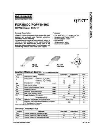
fqp3n80c fqpf3n80c.pdf
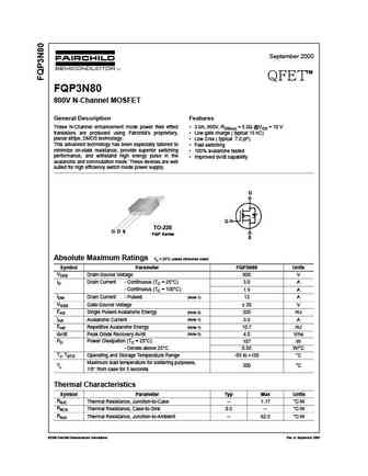
TM QFET FQP3N80C/FQPF3N80C 800V N-Channel MOSFET General Description Features These N-Channel enhancement mode power field effect 3.0A, 800V, RDS(on) = 4.8 @VGS = 10 V transistors are produced using Fairchild s proprietary, Low gate charge ( typical 13 nC) planar stripe, DMOS technology. Low Crss ( typical 5.5 pF) This advanced technology has been especially tailored t... See More ⇒
fqaf13n80.pdf
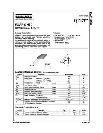
March 2001 TM QFET FQAF13N80 800V N-Channel MOSFET General Description Features These N-Channel enhancement mode power field effect 8.0A, 800V, RDS(on) = 0.75 @VGS = 10 V transistors are produced using Fairchild s proprietary, Low gate charge ( typical 68 nC) planar stripe, DMOS technology. Low Crss ( typical 30 pF) This advanced technology has been especially tailore... See More ⇒
fqpf3n80.pdf
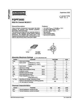
September 2000 TM QFET FQPF3N80 800V N-Channel MOSFET General Description Features These N-Channel enhancement mode power field effect 1.8A, 800V, RDS(on) = 5.0 @VGS = 10 V transistors are produced using Fairchild s proprietary, Low gate charge ( typical 15 nC) planar stripe, DMOS technology. Low Crss ( typical 7.0 pF) This advanced technology has been especially tail... See More ⇒
fqa13n80.pdf
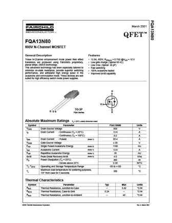
March 2001 TM QFET FQA13N80 800V N-Channel MOSFET General Description Features These N-Channel enhancement mode power field effect 12.6A, 800V, RDS(on) = 0.75 @VGS = 10 V transistors are produced using Fairchild s proprietary, Low gate charge ( typical 68 nC) planar stripe, DMOS technology. Low Crss ( typical 30 pF) This advanced technology has been especially tailore... See More ⇒
fqpf3n80cydtu.pdf
TM QFET FQP3N80C/FQPF3N80C 800V N-Channel MOSFET General Description Features These N-Channel enhancement mode power field effect 3.0A, 800V, RDS(on) = 4.8 @VGS = 10 V transistors are produced using Fairchild s proprietary, Low gate charge ( typical 13 nC) planar stripe, DMOS technology. Low Crss ( typical 5.5 pF) This advanced technology has been especially tailored t... See More ⇒
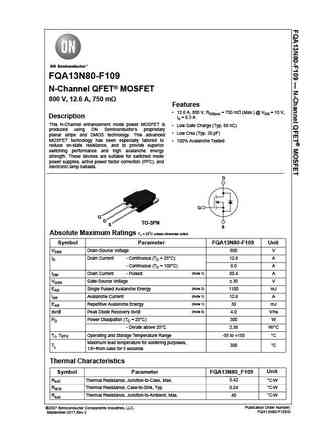
fqa13n80 f109.pdf
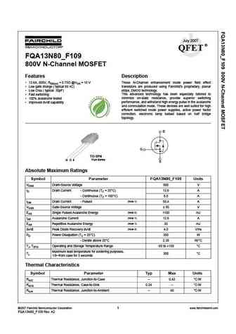
July 2007 QFET FQA13N80_F109 800V N-Channel MOSFET Features Description 12.6A, 800V, RDS(on) = 0.75 @VGS = 10 V These N-Channel enhancement mode power field effect Low gate charge ( typical 68 nC) transistors are produced using Fairchild s proprietary, planar stripe, DMOS technology. Low Crss ( typical 30pF) This advanced technology has been especially tailored to... See More ⇒
fqp3n80.pdf
September 2000 TM QFET FQP3N80 800V N-Channel MOSFET General Description Features These N-Channel enhancement mode power field effect 3.0A, 800V, RDS(on) = 5.0 @VGS = 10 V transistors are produced using Fairchild s proprietary, Low gate charge ( typical 15 nC) planar stripe, DMOS technology. Low Crss ( typical 7.0 pF) This advanced technology has been especially tailo... See More ⇒
ssp3n80a.pdf
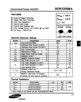
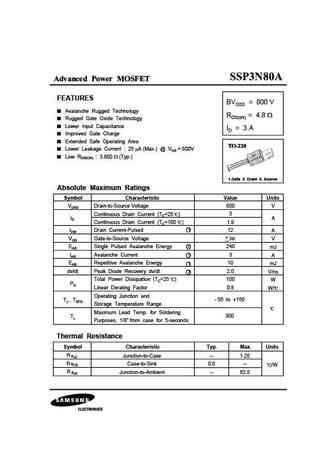
Advanced Power MOSFET FEATURES BVDSS = 800 V Avalanche Rugged Technology RDS(on) = 4.8 Rugged Gate Oxide Technology Lower Input Capacitance ID = 3 A Improved Gate Charge Extended Safe Operating Area Lower Leakage Current 25 A (Max.) @ VDS = 800V Low RDS(ON) 3.800 (Typ.) 1 2 3 1.Gate 2. Drain 3. Source Absolute Maximum Ratings Symbol Characteristic Value ... See More ⇒
sss3n80a.pdf
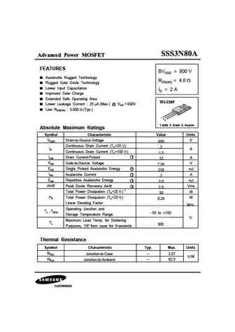
Advanced Power MOSFET FEATURES BVDSS = 800 V Avalanche Rugged Technology RDS(on) = 4.8 Rugged Gate Oxide Technology Lower Input Capacitance ID = 2 A Improved Gate Charge Extended Safe Operating Area Lower Leakage Current 25 A (Max.) @ VDS = 800V Low RDS(ON) 3.800 (Typ.) 1 2 3 1.Gate 2. Drain 3. Source Absolute Maximum Ratings Symbol Characteristic Value ... See More ⇒
ssu3n80a.pdf
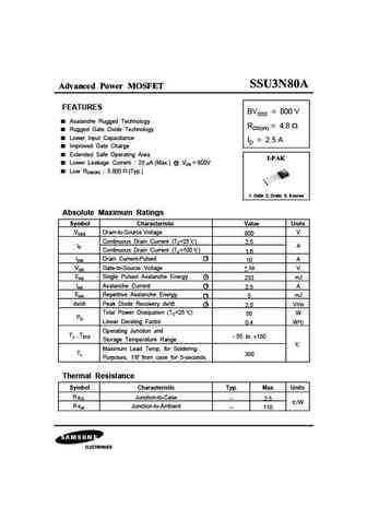
Advanced Power MOSFET FEATURES BVDSS = 800 V Avalanche Rugged Technology RDS(on) = 4.8 Rugged Gate Oxide Technology Lower Input Capacitance ID = 2.5 A Improved Gate Charge Extended Safe Operating Area Lower Leakage Current 25 A (Max.) @ VDS = 800V Low RDS(ON) 3.800 (Typ.) 1 2 3 1. Gate 2. Drain 3. Source Absolute Maximum Ratings Symbol Characteristic Value... See More ⇒
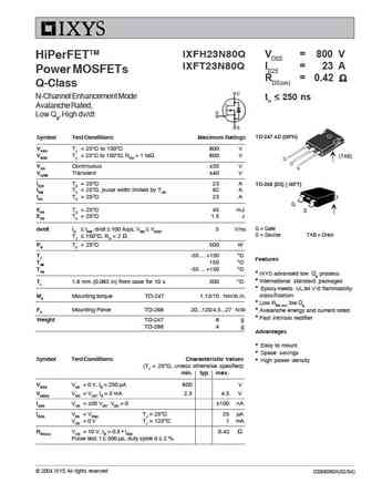
ixft23n80q.pdf
IXFH23N80Q VDSS = 800 V HiPerFETTM IXFT23N80Q ID25 = 23 A Power MOSFETs RDS(on) = 0.42 Q-Class N-Channel Enhancement Mode trr 250 ns Avalanche Rated, Low Qg, High dv/dt TO-247 AD (IXFH) Symbol Test Conditions Maximum Ratings VDSS TJ = 25 C to 150 C 800 V VDGR TJ = 25 C to 150 C; RGS = 1 M 800 V (TAB) VGS Continuous 30... See More ⇒
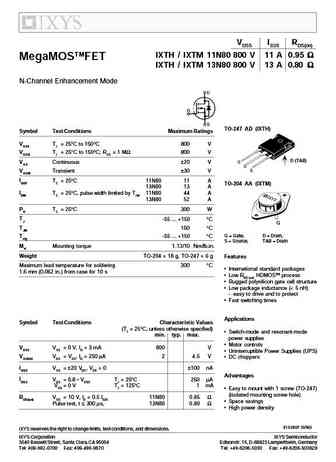
ixth11n80 ixtm11n80 ixth13n80 ixtm13n80.pdf
VDSS ID25 RDS(on) IXTH / IXTM 11N80 800 V 11 A 0.95 MegaMOSTMFET IXTH / IXTM 13N80 800 V 13 A 0.80 N-Channel Enhancement Mode TO-247 AD (IXTH) Symbol Test Conditions Maximum Ratings VDSS TJ = 25 C to 150 C 800 V VDGR TJ = 25 C to 150 C; RGS = 1 M 800 V D (TAB) VGS Continuous 20 V VGSM Transient 30 V ID25 TC = 25 C 11N80 11... See More ⇒
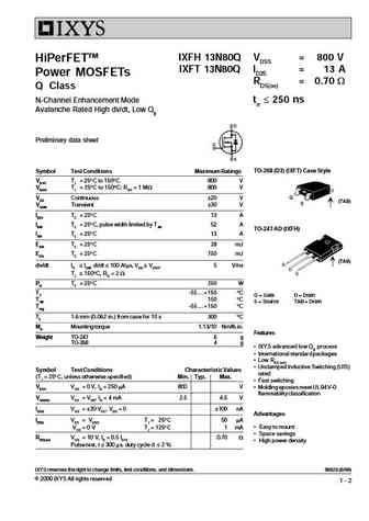
ixfh13n80q ixft13n80q.pdf
IXFH 13N80Q VDSS = 800 V HiPerFETTM IXFT 13N80Q ID25 = 13 A Power MOSFETs RDS(on) = 0.70 W Q Class N-Channel Enhancement Mode trr 250 ns Avalanche Rated High dv/dt, Low Qg Preliminary data sheet TO-268 (D3) (IXFT) Case Style Symbol Test Conditions Maximum Ratings VDSS TJ = 25 C to 150 C 800 V VDGR TJ = 25 C to 150 C; RGS = 1 MW 800 V G VGS Continuous 20 V (TAB) S VGSM ... See More ⇒
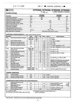
ixtm3n80 ixtm3n80a ixtm3n90 ixtm3n90a ixtp3n80 ixtp3n80a ixtp3n90 ixtp3n90a.pdf
... See More ⇒
ixfh11n80 ixfh13n80 ixfm11n80 ixfm13n80.pdf
VDSS ID25 RDS(on) HiPerFETTM IXFH/IXFM 11 N80 800 V 11 A 0.95 W Power MOSFETs IXFH/IXFM 13 N80 800 V 13 A 0.80 W trr 250 ns N-Channel Enhancement Mode High dv/dt, Low trr, HDMOSTM Family Symbol Test Conditions Maximum Ratings TO-247 AD (IXFH) VDSS TJ = 25 C to 150 C 800 V VDGR TJ = 25 C to 150 C; RGS = 1 MW 800 V VGS Continuous 20 V (TAB) VGSM Transient 30 V ID25 TC = 2... See More ⇒
fqa13n80-f109.pdf
FQA13N80-F109 N-Channel QFET MOSFET 800 V, 12.6 A, 750 m Features 12.6 A, 800 V, RDS(on) = 750 m (Max.) @ VGS = 10 V, Description ID = 6.3 A This N-Channel enhancement mode power MOSFET is Low Gate Charge (Typ. 68 nC) produced using ON Semiconductor s proprietary Low Crss (Typ. 30 pF) planar stripe and DMOS technology. This advanced MOSFET technology has be... See More ⇒
fqp3n80c fqpf3n80c.pdf
Is Now Part of To learn more about ON Semiconductor, please visit our website at www.onsemi.com Please note As part of the Fairchild Semiconductor integration, some of the Fairchild orderable part numbers will need to change in order to meet ON Semiconductor s system requirements. Since the ON Semiconductor product management systems do not have the ability to manage part nomenclatur... See More ⇒
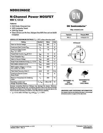
ndd03n80z.pdf
NDD03N80Z N Channel Power MOSFET 800 V, 4.5 W Features ESD Diode-Protected Gate 100% Avalanche Tested http //onsemi.com 100% Rg Tested These Devices are Pb-Free, Halogen Free/BFR Free and are RoHS V(BR)DSS RDS(ON) MAX Compliant 800 V 4.5 W @ 10 V ABSOLUTE MAXIMUM RATINGS (TC = 25 C unless otherwise noted) Rating Symbol Value Unit N-Channel Drain-to-Source Volta... See More ⇒
3n80l-ta3-t 3n80g-ta3-t 3n80l-tf3-t 3n80g-tf3-t 3n80l-tf1-t 3n80g-tf1-t 3n80l-tf2-t 3n80g-tf2-t 3n80l-tm3-t 3n80g-tm3-t 3n80l-tms4-r 3n80g-tms4-r 3n80l-tn3-r 3n80g-tn3-r.pdf
UNISONIC TECHNOLOGIES CO., LTD 3N80 Power MOSFET 3.0 Amps, 800Volts N-CHANNEL POWER MOSFET DESCRIPTION The UTC 3N80 provide excellent RDS(ON), low gate charge and operation with low gate voltages. This device is suitable for use as a load switch or in PWM applications. FEATURES * RDS(ON) ... See More ⇒
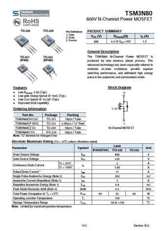
tsm3n80ch tsm3n80ci tsm3n80cp tsm3n80cz.pdf
TSM3N80 800V N-Channel Power MOSFET TO-220 ITO-220 PRODUCT SUMMARY Pin Definition 1. Gate VDS (V) RDS(on)( ) ID (A) 2. Drain 3. Source 800 4.2 @ VGS =10V 1.5 General Description The TSM3N80 N-Channel Power MOSFET is TO-251 TO-252 (IPAK) (DPAK) produced by new advance planar process. This advanced technology has been especially tailored to minimize on-state re... See More ⇒
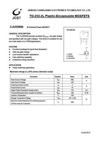
cju03n80.pdf
JIANGSU CHANGJIANG ELECTRONICS TECHNOLOGY CO., LTD TO-252-2L Plastic-Encapsulate MOSFETS CJU03N80 N-Channel Power MOSFET TO-252-2L GENERAL DESCRIPTION The CJU03N80 provide excellent RDS(ON), low gate charge and operation with low gate voltages. This device is suitable for use as a load switch or in PWM applications. FEATURE Excellent package for good heat dissipation ... See More ⇒
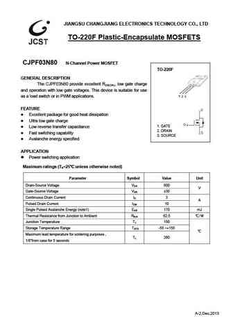
cjpf03n80.pdf
JIANGSU CHANGJIANG ELECTRONICS TECHNOLOGY CO., LTD TO-220F Plastic-Encapsulate MOSFETS CJPF03N80 N-Channel Power MOSFET TO-220F GENERAL DESCRIPTION The CJPF03N80 provide excellent RDS(ON), low gate charge and operation with low gate voltages. This device is suitable for use as a load switch or in PWM applications. FEATURE Excellent package for good heat dissipation Ul... See More ⇒
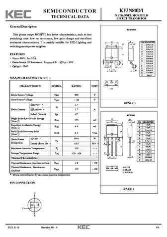
kf3n80d i.pdf
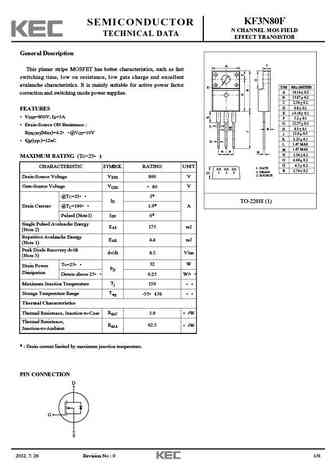
KF3N80D/I SEMICONDUCTOR N CHANNEL MOS FIELD TECHNICAL DATA EFFECT TRANSISTOR General Description KF3N80D This planar stripe MOSFET has better characteristics, such as fast switching time, low on resistance, low gate charge and excellent A K DIM MILLIMETERS avalanche characteristics. It is mainly suitable for LED Lighting and L C D _ A 6.60 + 0.20 switching mode power supplies. ... See More ⇒
kf3n80f.pdf
KF3N80F SEMICONDUCTOR N CHANNEL MOS FIELD TECHNICAL DATA EFFECT TRANSISTOR General Description C A This planar stripe MOSFET has better characteristics, such as fast switching time, low on resistance, low gate charge and excellent avalanche characteristics. It is mainly suitable for active power factor E DIM MILLIMETERS _ A 10.16 0.2 + correction and switching mode power supplie... See More ⇒
aod3n80.pdf
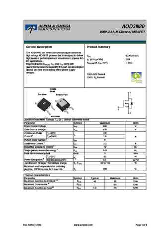
AOD3N80 800V,2.8A N-Channel MOSFET General Description Product Summary The AOD3N80 has been fabricated using an advanced high voltage MOSFET process that is designed to deliver VDS 900V@150 high levels of performance and robustness in popular AC- ID (at VGS=10V) 2.8A DC applications. RDS(ON) (at VGS=10V) ... See More ⇒
aotf3n80.pdf
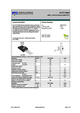
AOTF3N80 800V, 2.8A N-Channel MOSFET General Description Product Summary VDS 900V@150 The AOTF3N80 has been fabricated using an advanced high voltage MOSFET process that is designed to deliver ID (at VGS=10V) 2.8A high levels of performance and robustness in popular AC- RDS(ON) (at VGS=10V) ... See More ⇒
jcs3n80v jcs3n80r jcs3n80b jcs3n80s jcs3n80c jcs3n80f jcs3n80v.pdf
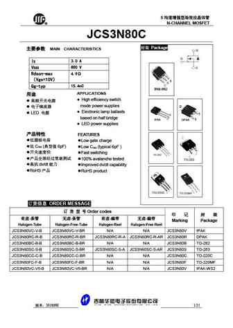
N R N-CHANNEL MOSFET JCS3N80C Package MAIN CHARACTERISTICS ID 3.0 A VDSS 800 V Rdson-max 4.9 Vgs=10V Qg-typ 15.4nC APPLICATIONS High efficiency switch mode power supplies Electronic lamp ballasts LED based on half bridge LE... See More ⇒
sdf03n80 sdp03n80.pdf
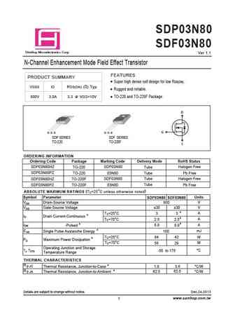
SDP03N80 SDF03N80 a S mHop Microelectronics C orp. Ver 1.1 N-Channel Enhancement Mode Field Effect Transistor FEATURES PRODUCT SUMMARY Super high dense cell design for low RDS(ON). VDSS ID RDS(ON) ( ) Typ Rugged and reliable. 800V 3.0A 3.3 @ VGS=10V TO-220 and TO-220F Package. D G G D S G D S SDP SERIES SDF SERIES TO-220 TO-220F S ORDERING INFORMATION Ordering Code Package M... See More ⇒
ssf3n80d.pdf
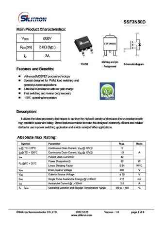
SSF3N80D Main Product Characteristics VDSS 800V RDS(on) 3.8 (typ.) ID 3A Marking and p in TO-252 Schematic diagram Assignment Features and Benefits Advanced MOSFET process technology Special designed for PWM, load switching and general purpose applications Ultra low on-resistance with low gate charge Fast switching and reverse body recovery ... See More ⇒
ssf3n80f.pdf
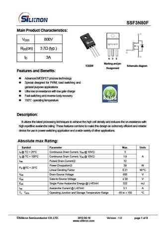
SSF3N80F Main Product Characteristics VDSS 800V RDS(on) 3.7 (typ.) ID 3A Marking a nd p in Sche ma ti c di agr a m TO220F Assignment Features and Benefits Advanced MOSFET process technology Special designed for PWM, load switching and general purpose applications Ultra low on-resistance with low gate charge Fast switching and reverse body recove... See More ⇒
brf3n80.pdf
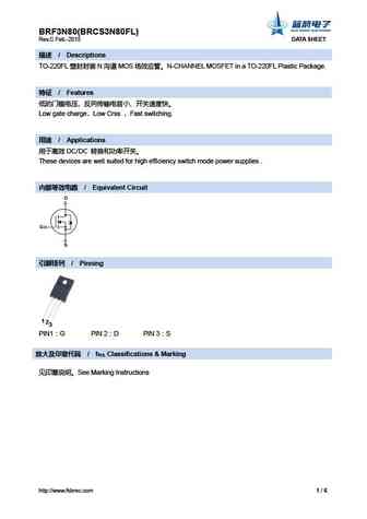
BRF3N80(BRCS3N80FL) Rev.C Feb.-2015 DATA SHEET / Descriptions TO-220FL N MOS N-CHANNEL MOSFET in a TO-220FL Plastic Package. / Features Low gate charge Low Crss Fast switching. / Applications DC/DC These devices are... See More ⇒
brd3n80.pdf
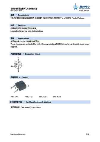
BRD3N80(BRCS3N80D) Rev.C Feb.-2015 DATA SHEET / Descriptions TO-252 N MOS N-CHANNEL MOSFET in a TO-252 Plastic Package. / Features , , Low gate charge, low crss, fast switching. / Applications DC/DC These devices are well suited for high... See More ⇒
bri3n80.pdf
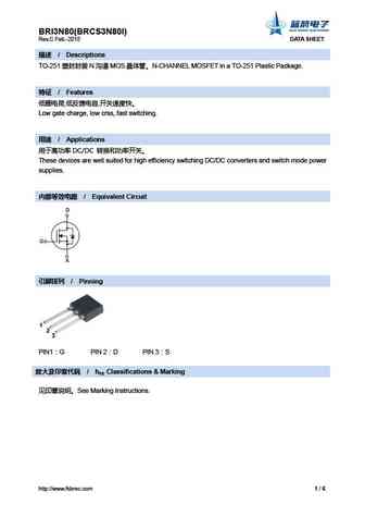
BRI3N80(BRCS3N80I) Rev.C Feb.-2015 DATA SHEET / Descriptions TO-251 N MOS N-CHANNEL MOSFET in a TO-251 Plastic Package. / Features , , Low gate charge, low crss, fast switching. / Applications DC/DC These devices are well suited for high ef... See More ⇒
3n80a 3n80af.pdf
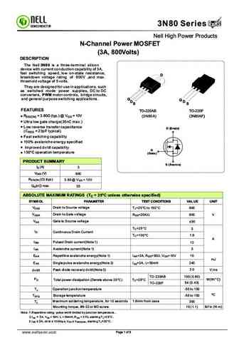
RoHS 3N80 Series RoHS SEMICONDUCTOR Nell High Power Products N-Channel Power MOSFET (3A, 800Volts) DESCRIPTION The Nell 3N80 is a three-terminal silicon device with current conduction capability of 3A, fast switching speed, low on-state resistance, D breakdown voltage rating of 800V ,and max. threshold voltage of 5 volts. They are designed for use in applications. such as sw... See More ⇒
cs3n80 arh.pdf
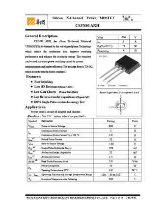
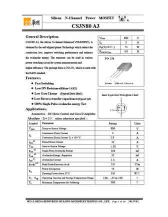
Silicon N-Channel Power MOSFET R CS3N80 ARH General Description VDSS 800 V CS3N80 ARH, the silicon N-channel Enhanced ID 3 A PD(TC=25 ) 75 W VDMOSFETs, is obtained by the self-aligned planar Technology RDS(ON)Typ 4 which reduce the conduction loss, improve switching performance and enhance the avalanche energy. The transistor can be used in various power sw... See More ⇒
cs3n80 a3.pdf
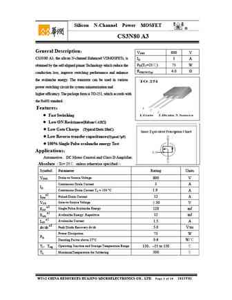
Silicon N-Channel Power MOSFET R CS3N80 A3 General Description VDSS 800 V CS3N80 A3, the silicon N-channel Enhanced VDMOSFETs, is ID 3 A PD(TC=25 ) 75 W obtained by the self-aligned planar Technology which reduce the RDS(ON)Typ 4.0 conduction loss, improve switching performance and enhance the avalanche energy. The transistor can be used in various power swit... See More ⇒
cs3n80 a8.pdf
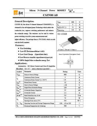
Silicon N-Channel Power MOSFET R CS3N80 A8 General Description VDSS 800 V CS3N80 A8, the silicon N-channel Enhanced VDMOSFETs, is ID 3 A PD(TC=25 ) 75 W obtained by the self-aligned planar Technology which reduce the RDS(ON)Typ 4.0 conduction loss, improve switching performance and enhance the avalanche energy. The transistor can be used in various power swit... See More ⇒
cs3n80f a9.pdf
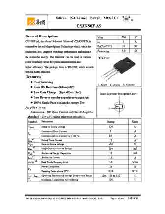
Silicon N-Channel Power MOSFET R CS3N80F A9 General Description VDSS 800 V CS3N80F A9, the silicon N-channel Enhanced VDMOSFETs, is ID 3 A PD(TC=25 ) 30 W obtained by the self-aligned planar Technology which reduce the RDS(ON)Typ 4.0 conduction loss, improve switching performance and enhance the avalanche energy. The transistor can be used in various power... See More ⇒
cs3n80 a4.pdf
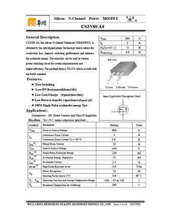
Silicon N-Channel Power MOSFET R CS3N80 A4 General Description VDSS 800 V CS3N80 A4, the silicon N-channel Enhanced VDMOSFETs, is ID 3 A PD(TC=25 ) 75 W obtained by the self-aligned planar Technology which reduce the RDS(ON)Typ 4.0 conduction loss, improve switching performance and enhance the avalanche energy. The transistor can be used in various power s... See More ⇒
ftk3n80p f d i.pdf
SEMICONDUCTOR FTK3N80P/F/D/I TECHNICAL DATA 3 Amps, 800 Volts Power MOSFET N-CHANNEL MOSFET I 1 TO - 251 DESCRIPTION The FTK 3N80 is a high voltage MOSFET and is designed to D 1 have better characteristics, such as fast switching time, low gate TO - 252 charge, low on-state resistance and have a high rugged avalanche characteristics. This power MOSFET is usually used at hig... See More ⇒
ftk3n80p f.pdf
SEMICONDUCTOR FTK3N80P / F TECHNICAL DATA Power MOSFET 3 Amps, 800 Volts N-CHANNEL MOSFET P 1 DESCRIPTION TO-220 The FTK 3N80 is a high voltage MOSFET and is designed to have better characteristics, such as fast switching time, low gate charge, low on-state resistance and have a high rugged avalanche characteristics. This power MOSFET is usually used at high speed F switchin... See More ⇒
kx3n80.pdf
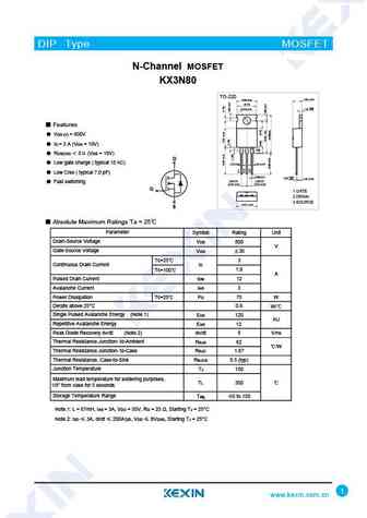
DIP Type MOSFET N-Channel MOSFET KX3N80 TO-220 9.90 0.20 4.50 0.20 (8.70) +0.10 3.60 0.10 1.30 0.05 Features VDS (V) = 800V ID = 3 A (VGS = 10V) RDS(ON) 5 (VGS = 10V) D Low gate charge ( typical 15 nC) 1.27 0.10 1.52 0.10 2 1 3 Low Crss ( typical 7.0 pF) 0.80 0.10 +0.10 0.50 0.05 2.40 0.20 2.54TYP 2.54TYP ... See More ⇒
svf3n80m svf3n80mj svf3n80f svf3n80d svf3n80t.pdf
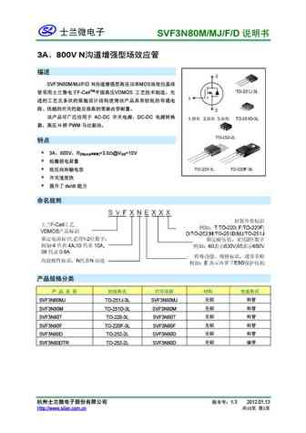
SVF3N80M/MJ/F/D 3A 800V N SVF3N80M/MJ/F/D N MOS F-CellTM VDMOS AC-DC... See More ⇒
msf3n80.pdf
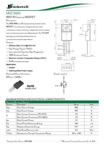
MSF3N80 800V N-Channel MOSFET Description The MSF3N80 is a N-channel enhancement-mode MOSFET , providing the designer with the best combination of fast switching, ruggedized device design, low on-resistance and cost effectiveness. The TO-220F package is universally preferred for all commercial-industrial applications Features RDS(on) (Max 4.8 )@VGS=10V Gate Char... See More ⇒
ms3n80.pdf
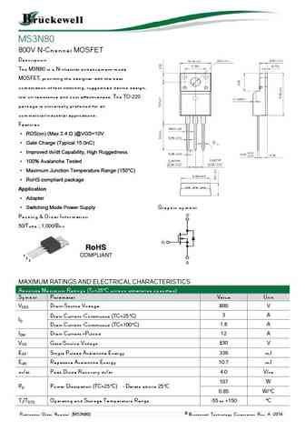
MS3N80 800V N-Channel MOSFET Description The M3N80 is a N-channel enhancement-mode MOSFET, providing the designer with the best combination of fast switching, ruggedized device design, low on-resistance and cost effectiveness. The TO-220 package is universally preferred for all commercial-industrial applications. Features RDS(on) (Max 2.4 )@VGS=10V Gate Charge (... See More ⇒
cs3n80fa9.pdf
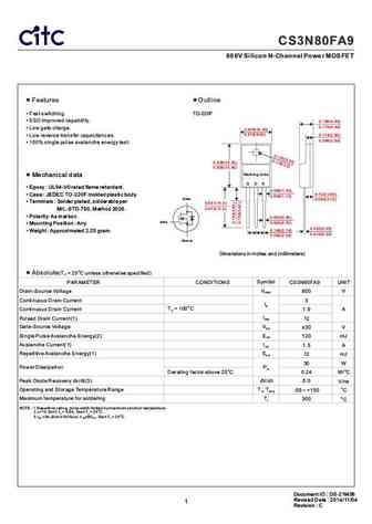
CS3N80FA9 800V Silicon N-Channel Power MOSFET Features Outline Fast switching. TO-220F ESD improved capability. 0.189(4.80) 0.173(4.40) Low gate charge. 0.409(10.40) 0.378(9.60) 0.114(2.90) Low reverse transfer capacitances. 0.098(2.50) 100% single pulse avalanche energy test. 0.638(16.20) 0.606(15.40) Marking code Mechanical data G D S Epox... See More ⇒
hy3n80t.pdf
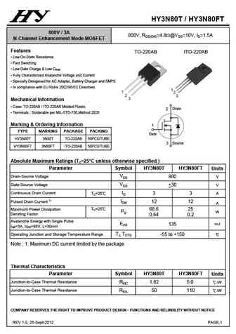
HY3N80T / HY3N80FT 800V / 3A 800V, RDS(ON)=4.8W@VGS=10V, ID=1.5A N-Channel Enhancement Mode MOSFET Features TO-220AB ITO-220AB Low On-State Resistance Fast Switching Low Gate Charge & Low CRSS Fully Characterized Avalanche Voltage and Current Specially Desigened for AC Adapter, Battery Charger and SMPS In compliance with EU RoHs 2002/95/EC Directives 1 ... See More ⇒
sw3n80c.pdf
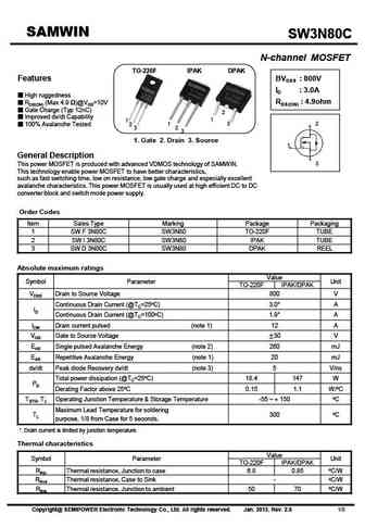
SAMWIN SW3N80C SW3N80C N-channel MOSFET TO-220F IPAK DPAK BVDSS 800V Features ID 3.0A High ruggedness RDS(ON) 4.9ohm RDS(ON) (Max 4.9 )@VGS=10V Gate Charge (Typ 12nC) 2 Improved dv/dt Capability 1 1 1 3 2 100% Avalanche Tested 2 3 2 3 1. Gate 2. Drain 3. Source 1 General Description 3 This power MOSFET is produced with advanced VDMOS technol... See More ⇒
swf13n80k.pdf
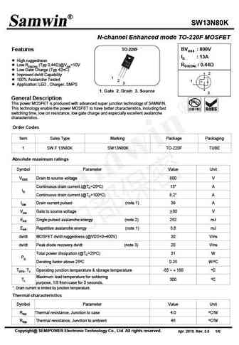
SW13N80K N-channel Enhanced mode TO-220F MOSFET TO-220F BVDSS 800V Features ID 13A High ruggedness RDS(ON) 0.44 Low RDS(ON) (Typ 0.44 )@VGS=10V Low Gate Charge (Typ 42nC) 2 Improved dv/dt Capability 1 100% Avalanche Tested 2 1 3 Application LED , Charger, SMPS 1. Gate 2. Drain 3. Source 3 General Description This powe... See More ⇒
swf3n80d swn3n80d swd3n80d.pdf
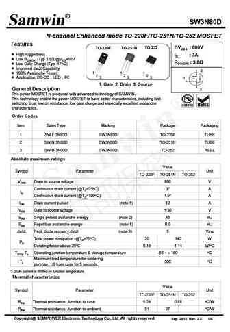
SW3N80D N-channel Enhanced mode TO-220F/TO-251N/TO-252 MOSFET Features TO-251N TO-252 BVDSS 800V TO-220F High ruggedness ID 3A Low RDS(ON) (Typ 3.8 )@VGS=10V RDS(ON) 3.8 Low Gate Charge (Typ 17nC) Improved dv/dt Capability 2 1 1 1 100% Avalanche Tested 2 2 2 Application DC-DC LED PC 3 3 3 1 1. Gate 2. Drain 3. Source ... See More ⇒
hfs3n80.pdf
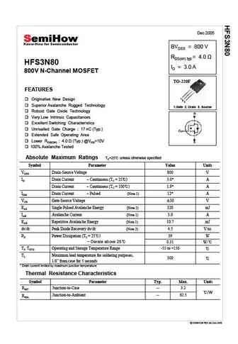
Dec 2005 BVDSS = 800 V RDS(on) typ HFS3N80 ID = 3.0 A 800V N-Channel MOSFET TO-220F FEATURES 1 1 Originative New Design 2 3 Superior Avalanche Rugged Technology 1.Gate 2. Drain 3. Source Robust Gate Oxide Technology Very Low Intrinsic Capacitances Excellent Switching Characteristics Unrivalled Gate Charge 17 nC (Typ.) Extended Safe Operating Area ... See More ⇒
hfd3n80.pdf
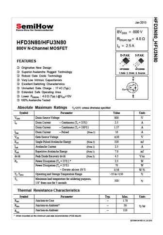
Jan 2013 BVDSS = 800 V RDS(on) typ HFD3N80/HFU3N80 ID = 2.5 A 800V N-Channel MOSFET D-PAK I-PAK 2 FEATURES 1 1 3 2 3 Originative New Design HFD3N80 HFU3N80 Superior Avalanche Rugged Technology 1.Gate 2. Drain 3. Source Robust Gate Oxide Technology Very Low Intrinsic Capacitances Excellent Switching Characteristics Unrivalled Gate Charge 17 nC (Typ.) ... See More ⇒
hfp3n80.pdf
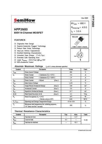
Dec 2005 BVDSS = 800 V RDS(on) typ = 4.0 HFP3N80 ID = 3.0 A 800V N-Channel MOSFET TO-220 FEATURES Originative New Design 1 2 3 Superior Avalanche Rugged Technology 1.Gate 2. Drain 3. Source Robust Gate Oxide Technology Very Low Intrinsic Capacitances Excellent Switching Characteristics Unrivalled Gate Charge 17 nC (Typ.) Unrivalled Gate Charge 17 nC (Typ ) Exten... See More ⇒
hfs3n80a.pdf
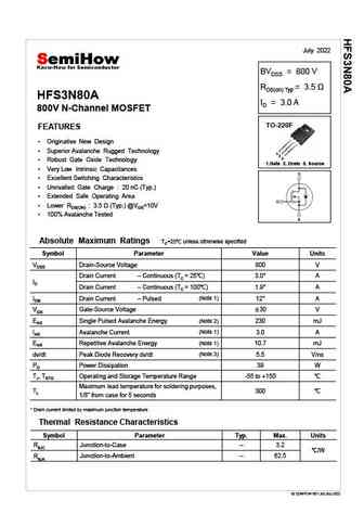
July 2022 BVDSS = 800 V RDS(on) Typ = 3.5 HFS3N80A ID = 3.0 A 800V N-Channel MOSFET TO-220F FEATURES Originative New Design Superior Avalanche Rugged Technology 1 2 3 Robust Gate Oxide Technology 1.Gate 2. Drain 3. Source Very Low Intrinsic Capacitances Excellent Switching Characteristics Unrivalled Gate Charge 20 nC (Typ.) Extended Safe Opera... See More ⇒
hfh13n80.pdf
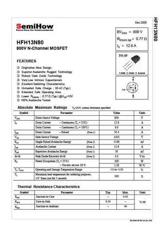
Dec 2005 BVDSS = 800 V RDS(on) typ HFH13N80 ID = 12.6 A 800V N-Channel MOSFET TO-3P FEATURES 1 Originative New Design 2 3 Superior Avalanche Rugged Technology 1.Gate 2. Drain 3. Source Robust Gate Oxide Technology Very Low Intrinsic Capacitances Excellent Switching Characteristics Unrivalled Gate Charge 68 nC (Typ.) Extended Safe Operating Area Lower RDS(... See More ⇒
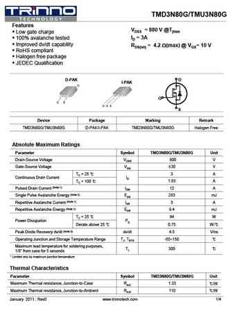
tmd3n80g tmu3n80g.pdf
TMD3N80G/TMU3N80G Features VDSS = 880 V @Tjmax Low gate charge ID = 3A 100% avalanche tested Improved dv/dt capability RDS(on) = 4.2 W(max) @ VGS= 10 V RoHS compliant Halogen free package JEDEC Qualification D-PAK D I-PAK G S Device Package Marking Remark TMD3N80G/TMU3N80G D-PAK/I-PAK TMD3N80G/TMU3N80G Halogen Free Absolute Maximum Ratings Parameter ... See More ⇒
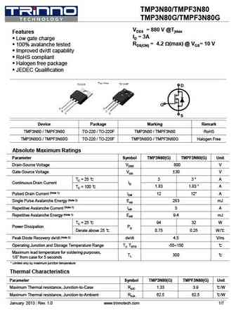
tmp3n80 tmpf3n80.pdf
TMP3N80/TMPF3N80 TMP3N80G/TMPF3N80G VDSS = 880 V @Tjmax Features ID = 3A Low gate charge RDS(ON) = 4.2 W(max) @ VGS= 10 V 100% avalanche tested Improved dv/dt capability RoHS compliant Halogen free package JEDEC Qualification D G S Device Package Marking Remark TMP3N80 / TMPF3N80 TO-220 / TO-220F TMP3N80 / TMPF3N80 RoHS TMP3N80G / TMPF3N... See More ⇒
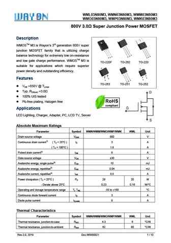
wml03n80m3 wmn03n80m3 wmm03n80m3 wmo03n80m3 wmp03n80m3 wmk03n80m3.pdf
WML03N80M3, W 80M3, WM M3 WMN03N8 MM03N80M WMO0 80M3, WM M3 03N80M3, WMP03N8 MK03N80M 800 Junction ET 0V 3.0 Super J n Power MOSFE Descrip ption WMOSTM M3 is Wayo neration 800 M on s 3rd gen 0V super junction MOSFET fa that is utilizing charge M amily S balance te or extremely esistance D echnology fo y low on-re S S G D D G G G T and low ga charge perf... See More ⇒
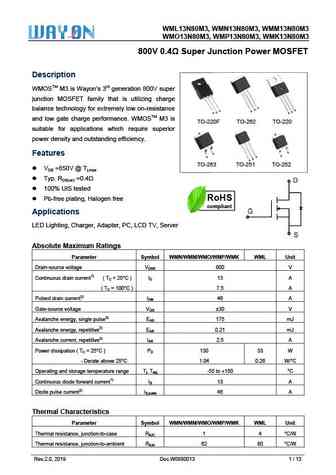
wml13n80m3 wmn13n80m3 wmm13n80m3 wmo13n80m3 wmp13n80m3 wmk13n80m3.pdf
WML13N80M3, W 80M3, WM M3 WMN13N8 MM13N80M WMO1 80M3, WM M3 13N80M3, WMP13N8 MK13N80M 800V 0.4 S T Super Junction Power MOSFET Descrip ption WMOSTM M3 is Wayo neration 800 M on s 3rd gen 0V super junction MOSFET fa that is utilizing charge M amily S balance te or extremely esistance D echnology fo y low on-re S S G D D G G G T and low ga charge performa... See More ⇒
cs3n80a8.pdf
Silicon N-Channel Power MOSFET R CS3N80 A8 General Description VDSS 800 V CS3N80 A8, the silicon N-channel Enhanced VDMOSFETs, is ID 3 A PD(TC=25 ) 75 W obtained by the self-aligned planar Technology which reduce the RDS(ON)Typ 4.0 conduction loss, improve switching performance and enhance the avalanche energy. The transistor can be used in various power swit... See More ⇒
cs3n80a4.pdf
Silicon N-Channel Power MOSFET R CS3N80 A4 General Description VDSS 800 V CS3N80 A4, the silicon N-channel Enhanced VDMOSFETs, is ID 3 A PD(TC=25 ) 75 W obtained by the self-aligned planar Technology which reduce the RDS(ON)Typ 4.0 conduction loss, improve switching performance and enhance the avalanche energy. The transistor can be used in various power s... See More ⇒
cs3n80a3.pdf
Silicon N-Channel Power MOSFET R CS3N80 A3 General Description VDSS 800 V CS3N80 A3, the silicon N-channel Enhanced VDMOSFETs, is ID 3 A PD(TC=25 ) 75 W obtained by the self-aligned planar Technology which reduce the RDS(ON)Typ 4.0 conduction loss, improve switching performance and enhance the avalanche energy. The transistor can be used in various power s... See More ⇒
cs3n80bf cs3n80bp cs3n80bu cs3n80bl cs3n80bk.pdf
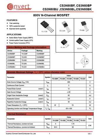
CS3N80BF, CS3N80BP nvert Suzhou Convert Semiconductor Co ., Ltd. CS3N80BU ,CS3N80BL,CS3N80BK 800V N-Channel MOSFET FEATURES Fast switching 100% avalanche tested Improved dv/dt capability APPLICATIONS Switch Mode Power Supply (SMPS) Uninterruptible Power Supply (UPS) Power Factor Correction (PFC) Device Marking and Package Information Device Package Marking... See More ⇒
spd3n80g.pdf
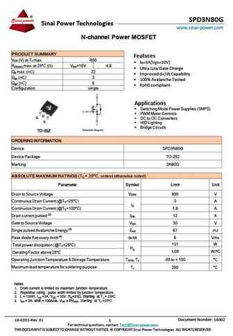
SPD3N80G Sinai Power Technologies www.sinai-power.com N-channel Power MOSFET PRODUCT SUMMARY Features V (V) at T max. 850 DS J ID=3A(Vgs=10V) R max. at 25oC ( ) V =10V 4.8 DS(on) GS Ultra Low Gate Charge Q max. (nC) 22 g Improved dv/dt Capability Q (nC) 3 gs 100% Avalanche Tested Q (nC) 6 gd RoHS compliant Configuration single Applic... See More ⇒
hm3n80.pdf
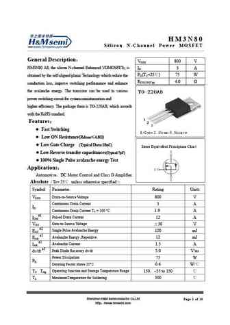
HM3N80 Si l i con N- Channel Power MOSFET General Description VDSS 800 V HM3N80 A8, the silicon N-channel Enhanced VDMOSFETs, is ID 3 A PD(TC=25 ) 75 W obtained by the self-aligned planar Technology which reduce the RDS(ON)Typ 4.0 conduction loss, improve switching performance and enhance the avalanche energy. The transistor can be used in various power switching c... See More ⇒
sfp086n80cc2 sfb083n80cc2.pdf
SFP086N80CC2, SFB083N80CC2 N-MOSFET 80V, 6.6m , 100A Features Product Summary Extremely low on-resistance RDS(on) VDS 80V Excellent QgxRDS(on) product(FOM) RDS(on) 6.6m Qualified according to JEDEC criteria ID 100A 100% DVDS Tested Applications 100% Avalanche Tested Motor control and drive 100% Avalanche Tested 100% Avalanche Tested 100% Avalanche Tested ... See More ⇒
sfp120n80a sfb120n80a sfp066n80ac3 sfb063n80ac3.pdf
SFP120N80A,SFB120N80A SFP066N80AC3,SFB063N80AC3 N-MOSFET 80V, 5.5m , 120A Features Product Summary Enhancement Mode VDS 80V Very Low On-Resistance RDS(on) 5.5m Fast Switching ID 120A 100% DVDS Tested Applications 100% Avalanche Tested Motor control and drive 100% Avalanche Tested 100% Avalanche Tested 100% Avalanche Tested 100% Avalanche Tested 100... See More ⇒
sfp066n80c3 sfb063n80c3.pdf
SFP066N80C3,SFB063N80C3 N-MOSFET 80V, 5.5m , 105A Features Product Summary Enhancement Mode VDS 80V Very Low On-Resistance RDS(on) 5.5m Fast Switching ID 105A 100% DVDS Tested Applications 100% Avalanche Tested Motor control and drive 100% Avalanche Tested 100% Avalanche Tested 100% Avalanche Tested 100% Avalanche Tested 100% Avalanche Tested Batt... See More ⇒
aod3n80.pdf
INCHANGE Semiconductor isc N-Channel MOSFET Transistor AOD3N80 FEATURES With TO-252(DPAK) packaging High speed switching Easy to use 100% avalanche tested Minimum Lot-to-Lot variations for robust device performance and reliable operation APPLICATIONS Power supply DC-DC converters Motor control Switching applications ABSOLUTE MAXIMUM RATINGS(T =25 ) a SY... See More ⇒
aotf3n80.pdf
isc N-Channel MOSFET Transistor AOTF3N80 FEATURES Drain Current I = 2.8A@ T =25 D C Drain Source Voltage- V =800V(Min) DSS Static Drain-Source On-Resistance R =4.8 (Max) DS(on) 100% avalanche tested Minimum Lot-to-Lot variations for robust device performance and reliable operation DESCRIPTION Designed for use in switch mode power supplies and general purpos... See More ⇒
stf23n80k5.pdf
isc N-Channel MOSFET Transistor STF23N80K5 FEATURES Drain Current I = 16A@ T =25 D C Drain Source Voltage V = 800V(Min) DSS Static Drain-Source On-Resistance R = 0.28 (Max) @ V = 10V DS(on) GS 100% avalanche tested Minimum Lot-to-Lot variations for robust device performance and reliable operation DESCRIPTION motor drive, DC-DC converter, power switch and sol... See More ⇒
Detailed specifications: 2N90, 3N90, 4N90, 5N90, 6N90, 7N90, 1N80, 2N80, IRF630, 4N80, 5N80, 6N80, 7N80, 8N80, 9N80, 10N80, 12N80
Keywords - 3N80 MOSFET specs
3N80 cross reference
3N80 equivalent finder
3N80 pdf lookup
3N80 substitution
3N80 replacement
Step-by-step guide to finding a MOSFET replacement. Cross-reference parts and ensure compatibility for your repair or project.
🌐 : EN ES РУ
LIST
Last Update
MOSFET: ASU70R600E | ASU65R850E | ASU65R550E | ASU65R350E | ASR65R120EFD | ASR65R046EFD | ASQ65R046EFD | ASM65R280E | ASM60R330E | ASE70R950E
Popular searches
2n1305 | 2sc5242 | irf540 equivalent | mp1620 transistor equivalent | 2sc945 transistor | c2073 transistor | ac176 transistor | mpsa20
