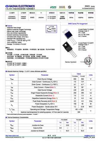
8N65 Specs and Replacement
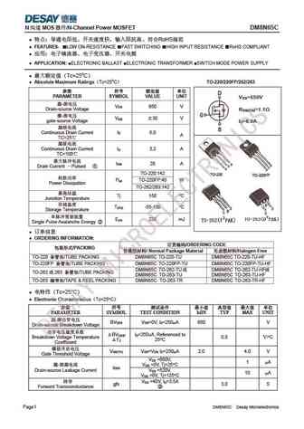
Type Designator: 8N65
Type of Transistor: MOSFET
Type of Control Channel: N-Channel
Absolute Maximum Ratings
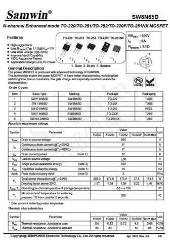
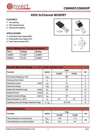
Pd ⓘ - Maximum Power Dissipation: 147 W
|Vds|ⓘ - Maximum Drain-Source Voltage: 650 V
|Vgs|ⓘ - Maximum Gate-Source Voltage: 30 V
|Id| ⓘ - Maximum Drain Current: 8 A
Tj ⓘ - Maximum Junction Temperature: 150 °C
Electrical Characteristics
tr ⓘ - Rise Time: 60.5 nS
Cossⓘ - Output Capacitance: 105 pF
RDSonⓘ - Maximum Drain-Source On-State Resistance: 1 Ohm
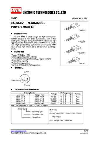
Package: TO-220 TO-262 TO-220F TO-220F1
8N65 substitution
- MOSFET ⓘ Cross-Reference Search
8N65 datasheet
8n65.pdf
UNISONIC TECHNOLOGIES CO., LTD 8N65 Power MOSFET 8A, 650V N-CHANNEL POWER MOSFET DESCRIPTION The UTC 8N65 is a high voltage and high current power MOSFET designed to have better characteristics, such as fast switching time, low gate charge, low on-state resistance and high rugged avalanche characteristics. This power MOSFET is usually used in high speed switching application... See More ⇒
8n65.pdf
INCHANGE Semiconductor isc N-Channel Mosfet Transistor 8N65 FEATURES Drain Current I = 8A@ T =25 D C Drain Source Voltage- V = 650V(Min) DSS Static Drain-Source On-Resistance R = 1.4 (Max) DS(on) Avalanche Energy Specified Fast Switching Minimum Lot-to-Lot variations for robust device performance and reliable operation DESCRITION High efficiency switch... See More ⇒
kps8n65f.pdf
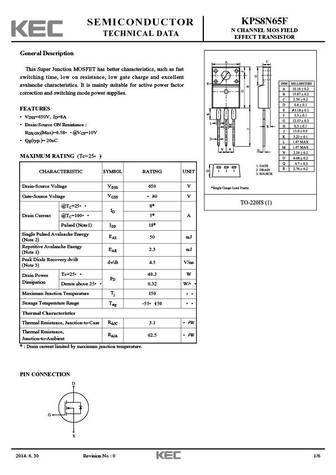
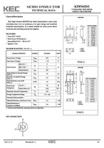
KPS8N65F SEMICONDUCTOR N CHANNEL MOS FIELD TECHNICAL DATA EFFECT TRANSISTOR General Description This Super Junction MOSFET has better characteristics, such as fast switching time, low on resistance, low gate charge and excellent avalanche characteristics. It is mainly suitable for active power factor correction and switching mode power supplies. FEATURES VDSS=650V, ID=8A Drain... See More ⇒
stw88n65m5.pdf
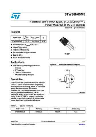
STW88N65M5 N-channel 650 V, 0.024 typ., 84 A, MDmesh V Power MOSFET in TO-247 package Datasheet production data Features VDSS Order code @Tjmax. RDS(on) max. ID STW88N65M5 710 V ... See More ⇒
stl38n65m5.pdf
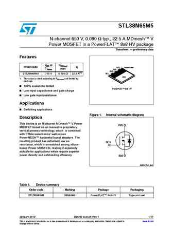
STL38N65M5 N-channel 650 V, 0.090 typ., 22.5 A MDmesh V Power MOSFET in a PowerFLAT 8x8 HV package Datasheet preliminary data Features VDS @ RDS(on) Order code ID S(2) Bottom view TJmax max S(2) S(2) G(1) STL38N65M5 710 V 0.105 22.5 A(1) D(3) 1. The value is rated according to Rthj-case and limited by package. 100% avalanche tested PowerFLAT 8x8 HV ... See More ⇒
stb28n65m2 stf28n65m2 stp28n65m2 stw28n65m2.pdf
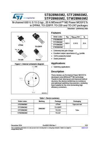
STB28N65M2, STF28N65M2, STP28N65M2, STW28N65M2 N-channel 650 V, 0.15 typ., 20 A MDmesh M2 Power MOSFETs in D PAK, TO-220FP, TO-220 and TO-247 packages Datasheet - preliminary data Features TAB Order codes VDS RDS(on) max ID STB28N65M2 3 3 STF28N65M2 1 2 650 V 0.18 20 A 1 STP28N65M2 D2PAK TO-220FP STW28N65M2 TAB Extremely low gate charge Excellent output... See More ⇒
stb18n65m5 std18n65m5.pdf
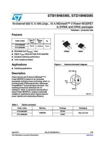
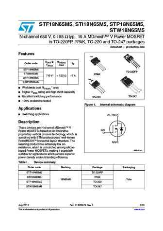
STB18N65M5, STD18N65M5 N-channel 650 V, 0.198 typ., 15 A MDmesh V Power MOSFET in D PAK and DPAK packages Datasheet production data Features VDSS @ RDS(on) Order codes ID TAB TJmax max TAB STB18N65M5 710 V ... See More ⇒
stfu18n65m2.pdf
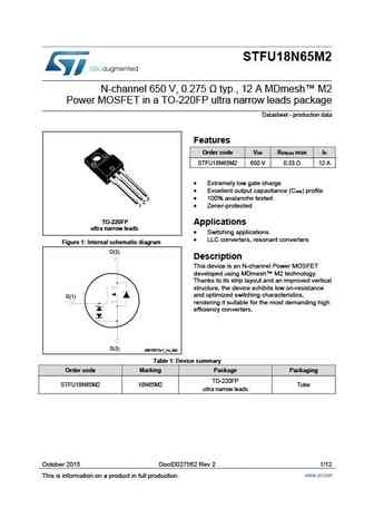
STFU18N65M2 N-channel 650 V, 0.275 typ., 12 A MDmesh M2 Power MOSFET in a TO-220FP ultra narrow leads package Datasheet - production data Features Order code V R max I DS DS(on) D STFU18N65M2 650 V 0.33 12 A Extremely low gate charge Excellent output capacitance (C ) profile oss 100% avalanche tested 3 2 1 Zener-protected TO-220FP Application... See More ⇒
stf18n65m2.pdf
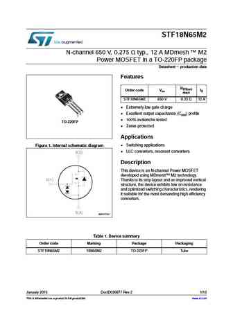
STF18N65M2 N-channel 650 V, 0.275 typ., 12 A MDmesh M2 Power MOSFET in a TO-220FP package Datasheet - production data Features RDS(on) Order code VDS ID max STF18N65M2 650 V 0.33 12 A Extremely low gate charge 3 2 Excellent output capacitance (Coss) profile 1 100% avalanche tested TO-220FP Zener-protected Applications Switching applications F... See More ⇒
ste88n65m5.pdf
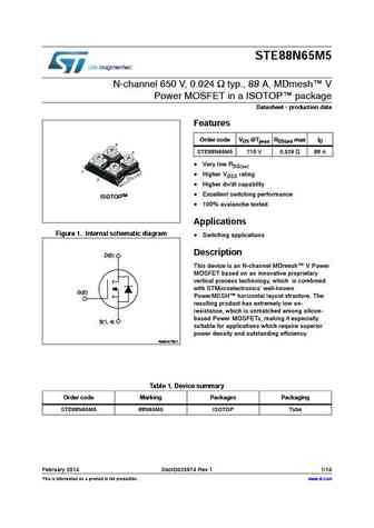
STE88N65M5 N-channel 650 V, 0.024 typ., 88 A, MDmesh V Power MOSFET in a ISOTOP package Datasheet - production data Features Order code VDS @Tjmax RDS(on) max ID STE88N65M5 710 V 0.029 88 A Very low RDS(on) Higher VDSS rating Higher dv/dt capability Excellent switching performance ISOTOPTM 100% avalanche tested Applications Figure 1. Internal sch... See More ⇒
sti18n65m2 stp18n65m2.pdf
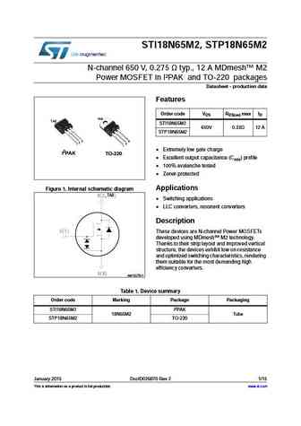
STI18N65M2, STP18N65M2 N-channel 650 V, 0.275 typ., 12 A MDmesh M2 Power MOSFET in I PAK and TO-220 packages Datasheet - production data Features Order code VDS RDS(on) max ID TAB TAB STI18N65M2 650V 0.33 12 A STP18N65M2 3 3 2 2 1 1 Extremely low gate charge I2PAK TO-220 Excellent output capacitance (Coss) profile 100% avalanche tested Zener-prote... See More ⇒
stl18n65m2.pdf
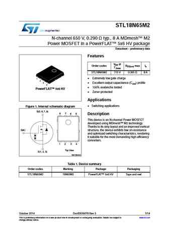
STL18N65M2 N-channel 650 V, 0.290 typ., 8 A MDmesh M2 Power MOSFET in a PowerFLAT 5x6 HV package Datasheet - preliminary data Features VDS @ Order codes TJmax RDS(on) max ID STL18N65M2 715 V 0.365 8 A Extremely low gate charge 1 2 3 Excellent output capacitance (Coss) profile 4 100% avalanche tested PowerFLAT 5x6 HV Zener-protected Applicatio... See More ⇒
stb38n65m5 stf38n65m5 stp38n65m5 stw38n65m5.pdf
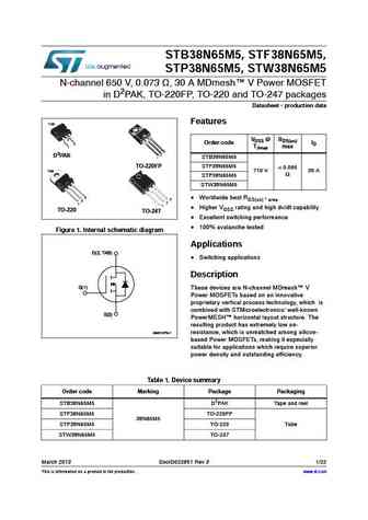
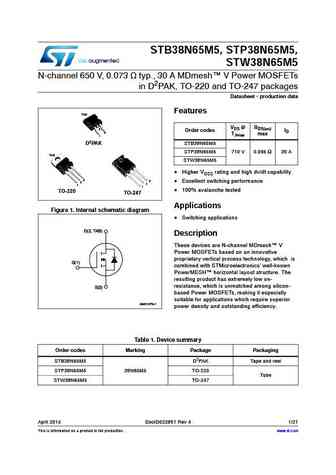
STB38N65M5, STF38N65M5, STP38N65M5, STW38N65M5 N-channel 650 V, 0.073 , 30 A MDmesh V Power MOSFET in D2PAK, TO-220FP, TO-220 and TO-247 packages Datasheet - production data Features TAB 2 VDSS @ RDS(on) 3 Order code ID 1 TJmax max 3 2 D2PAK STB38N65M5 1 TO-220FP STF38N65M5 ... See More ⇒
stb38n65m5 stp38n65m5 stw38n65m5.pdf
STB38N65M5, STP38N65M5, STW38N65M5 N-channel 650 V, 0.073 typ., 30 A MDmesh V Power MOSFETs in D2PAK, TO-220 and TO-247 packages Datasheet - production data Features TAB VDS @ RDS(on) 2 Order codes ID 3 TJmax max 1 STB38N65M5 D2PAK STP38N65M5 710 V 0.095 30 A TAB STW38N65M5 Higher VDSS rating and high dv/dt capability 3 3 Excellent switching performance... See More ⇒
stwa88n65m5.pdf
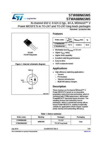
STW88N65M5 STWA88N65M5 N-channel 650 V, 0.024 typ., 84 A, MDmesh V Power MOSFETs in TO-247 and TO-247 long leads packages Datasheet - production data Features VDSS Order codes @Tjmax. RDS(on) max. ID STW88N65M5 710 V 0.029 84 A STWA88N65M5 3 2 1 Worldwide best RDS(on) in TO-247 TO-247 Higher VDSS rating TO-247 long leads Higher dv/dt capability Ex... See More ⇒
stl18n65m5.pdf
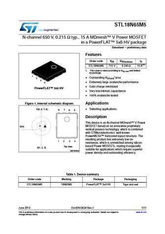
STL18N65M5 N-channel 650 V, 0.215 typ., 15 A MDmesh V Power MOSFET in a PowerFLAT 5x6 HV package Datasheet - preliminary data Features Order code VDS RDS(on)max. ID STL18N65M5 710 V 0.240 15 A(1) 1. The value is rated according to Rthj-case and limited by package. 1 Outstanding RDS(on)*area 2 3 Extremely large avalanche performance 4 Gate charge minimize... See More ⇒
stf18n65m5 sti18n65m5 stp18n65m5 stw18n65m5.pdf
STF18N65M5, STI18N65M5, STP18N65M5, STW18N65M5 N-channel 650 V, 0.198 typ., 15 A MDmesh V Power MOSFET in TO-220FP, I PAK, TO-220 and TO-247 packages Datasheet production data Features TAB VDSS @ RDS(on) Order code ID TJmax max 3 2 1 3 STF18N65M5 2 1 TO-220FP STI18N65M5 I PAK 710 V ... See More ⇒
stw88n65m5 stwa88n65m5.pdf
STW88N65M5 STWA88N65M5 N-channel 650 V, 0.024 typ., 84 A, MDmesh V Power MOSFETs in TO-247 and TO-247 long leads packages Datasheet - production data Features VDSS Order codes @Tjmax. RDS(on) max. ID STW88N65M5 710 V 0.029 84 A STWA88N65M5 3 2 1 Worldwide best RDS(on) in TO-247 TO-247 Higher VDSS rating TO-247 long leads Higher dv/dt capability Ex... See More ⇒
stw78n65m5.pdf
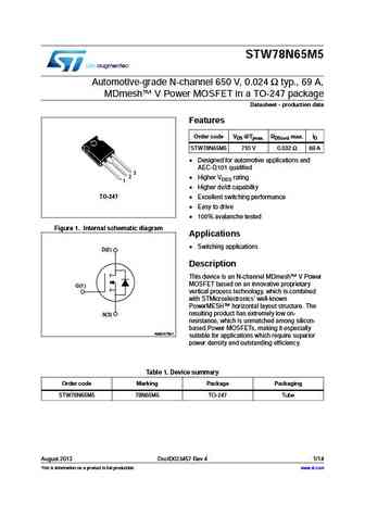
STW78N65M5 Automotive-grade N-channel 650 V, 0.024 typ., 69 A, MDmesh V Power MOSFET in a TO-247 package Datasheet - production data Features Order code VDS @Tjmax. RDS(on) max. ID STW78N65M5 710 V 0.032 69 A Designed for automotive applications and AEC-Q101 qualified 3 2 Higher VDSS rating 1 Higher dv/dt capability TO-247 Excellent switching performan... See More ⇒
stfw38n65m5.pdf
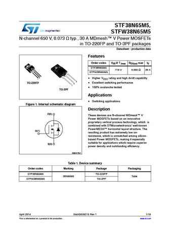
STF38N65M5, STFW38N65M5 N-channel 650 V, 0.073 typ., 30 A MDmesh V Power MOSFETs in TO-220FP and TO-3PF packages Datasheet - production data Features Order codes VDS@ TJmax RDS(on) max ID STF38N65M5 710 V 0.095 30 A STFW38N65M5 1 1 1 3 2 Higher VDSS rating and high dv/dt capability 1 3 TO-220FP Excellent switching performance 2 1 100% avalanche teste... See More ⇒
tk28n65w5.pdf
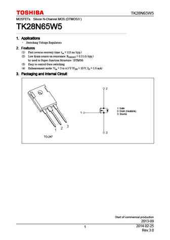
TK28N65W5 MOSFETs Silicon N-Channel MOS (DTMOS ) TK28N65W5 TK28N65W5 TK28N65W5 TK28N65W5 1. Applications 1. Applications 1. Applications 1. Applications Switching Voltage Regulators 2. Features 2. Features 2. Features 2. Features (1) Fast reverse recovery time trr = 115 ns (typ.) (2) Low drain-source on-resistance RDS(ON) = 0.11 (typ.) by used to Super Junction Str... See More ⇒
tk28n65w.pdf
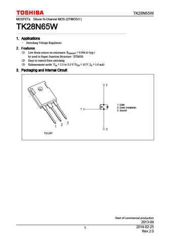
TK28N65W MOSFETs Silicon N-Channel MOS (DTMOS ) TK28N65W TK28N65W TK28N65W TK28N65W 1. Applications 1. Applications 1. Applications 1. Applications Switching Voltage Regulators 2. Features 2. Features 2. Features 2. Features (1) Low drain-source on-resistance RDS(ON) = 0.094 (typ.) by used to Super Junction Structure DTMOS (2) Easy to control Gate switching (3) E... See More ⇒
dmg8n65sct.pdf
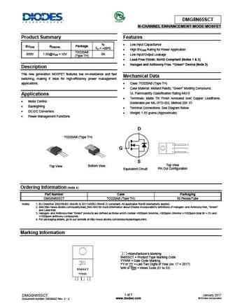
DMG8N65SCT N-CHANNEL ENHANCEMENT MODE MOSFET Product Summary Features ID Low Input Capacitance BVDSS RDS(ON) Package TC = +25 C High BVDSS Rating for Power Application TO220AB 650V 1.3 @VGS = 10V 8A Low Input/Output Leakage (Type TH) Lead-Free Finish; RoHS Compliant (Notes 1 & 2) Halogen and Antimony Free. Green Device (Note 3) Description... See More ⇒
ika08n65h5.pdf
IGBT High speed 5 IGBT in TRENCHSTOPTM 5 technology copacked with RAPID 1 fast and soft antiparallel diode IKA08N65H5 650V DuoPack IGBT and Diode High speed switching series fifth generation Data sheet Industrial Power Control IKA08N65H5 High speed switching series fifth generation High speed 5 IGBT in TRENCHSTOPTM 5 technology copacked with RAPID 1 fast and soft antiparallel diode ... See More ⇒
ika08n65et6.pdf
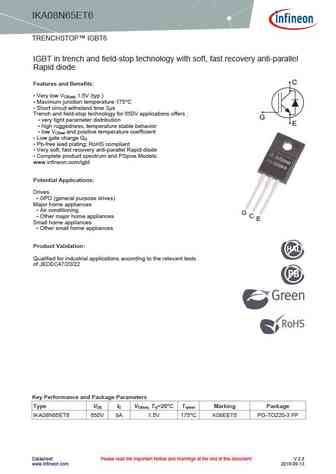
IKA08N65ET6 TRENCHSTOP IGBT6 IGBT in trench and field-stop technology with soft, fast recovery anti-parallel Rapid diode C Features and Benefits Very low V 1.5V (typ.) CE(sat) Maximum junction temperature 175 C Short circuit withstand time 3 s Trench and field-stop technology for 650V applications offers G very tight parameter distribution E high rugg... See More ⇒
ikp08n65h5.pdf
IGBT High speed 5 IGBT in TRENCHSTOPTM 5 technology copacked with RAPID 1 fast and soft antiparallel diode IKP08N65H5 650V DuoPack IGBT and Diode High speed switching series fifth generation Data sheet Industrial Power Control IKP08N65H5 High speed switching series fifth generation High speed 5 IGBT in TRENCHSTOPTM 5 technology copacked with RAPID 1 fast and soft antiparallel diode ... See More ⇒
ika08n65f5.pdf
IGBT High speed 5 FAST IGBT in TRENCHSTOPTM 5 technology copacked with RAPID 1 fast and soft antiparallel diode IKA08N65F5 650V DuoPack IGBT and Diode High speed switching series fifth generation Data sheet Industrial Power Control IKA08N65F5 High speed switching series fifth generation High speed 5 FAST IGBT in TRENCHSTOPTM 5 technology copacked with RAPID 1 fast and soft antiparal... See More ⇒
ikp08n65f5.pdf
IGBT High speed 5 FAST IGBT in TRENCHSTOPTM 5 technology copacked with RAPID 1 fast and soft antiparallel diode IKP08N65F5 650V DuoPack IGBT and Diode High speed switching series fifth generation Data sheet Industrial Power Control IKP08N65F5 High speed switching series fifth generation High speed 5 FAST IGBT in TRENCHSTOPTM 5 technology copacked with RAPID 1 fast and soft antiparal... See More ⇒
ikp28n65es5.pdf
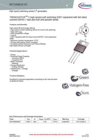
IKP28N65ES5 High speed switching series 5 th generation TRENCHSTOPTM 5 high speed soft switching IGBT copacked with full rated current RAPID 1 fast and soft anti parallel diode C Features and Benefits High speed S5 technology offering High speed smooth switching device for hard & soft switching Very Low V CEsat 650V breakdown voltage G Low Q G E IGBT copacked... See More ⇒
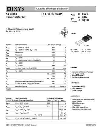
ixth48n65x2.pdf
Advance Technical Information X2-Class VDSS = 650V IXTH48N65X2 Power MOSFET ID25 = 48A RDS(on) 68m N-Channel Enhancement Mode Avalanche Rated TO-247 G D Symbol Test Conditions Maximum Ratings S D (Tab) VDSS TJ = 25 C to 150 C 650 V G = Gate D = Drain VDGR TJ = 25 C to 150 C, RGS = 1M 650 V S = Source Tab = Drain VGSS Continu... See More ⇒
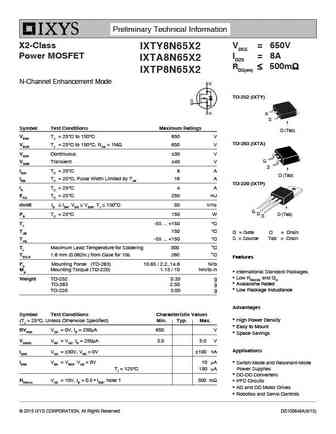
ixta8n65x2 ixtp8n65x2 ixty8n65x2.pdf
Preliminary Technical Information X2-Class VDSS = 650V IXTY8N65X2 Power MOSFET ID25 = 8A IXTA8N65X2 RDS(on) 500m IXTP8N65X2 N-Channel Enhancement Mode TO-252 (IXTY) G S Symbol Test Conditions Maximum Ratings D (Tab) VDSS TJ = 25 C to 150 C 650 V TO-263 (IXTA) VDGR TJ = 25 C to 150 C, RGS = 1M 650 V VGSS Continuous 30 V G... See More ⇒
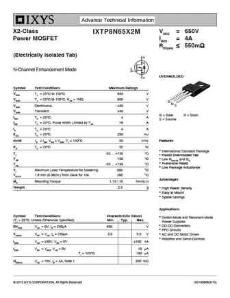
ixtp8n65x2m.pdf
Advance Technical Information X2-Class VDSS = 650V IXTP8N65X2M Power MOSFET ID25 = 4A RDS(on) 550m (Electrically Isolated Tab) N-Channel Enhancement Mode OVERMOLDED Symbol Test Conditions Maximum Ratings VDSS TJ = 25 C to 150 C 650 V VDGR TJ = 25 C to 150 C, RGS = 1M 650 V G D S VGSS Continuous 30 V VGSM Transient 40 V ... See More ⇒
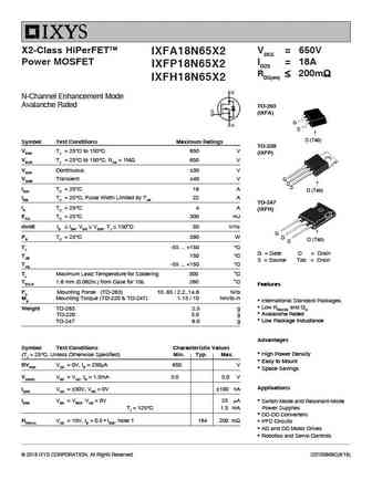
ixfa18n65x2 ixfp18n65x2 ixfh18n65x2.pdf
X2-Class HiPerFETTM VDSS = 650V IXFA18N65X2 Power MOSFET ID25 = 18A IXFP18N65X2 RDS(on) 200m IXFH18N65X2 N-Channel Enhancement Mode Avalanche Rated TO-263 (IXFA) G S D (Tab) Symbol Test Conditions Maximum Ratings TO-220 VDSS TJ = 25 C to 150 C 650 V (IXFP) VDGR TJ = 25 C to 150 C, RGS = 1M 650 V VGSS Continuous 30 V VGS... See More ⇒
18n65.pdf
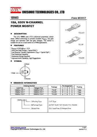
UNISONIC TECHNOLOGIES CO., LTD 18N65 Power MOSFET 18A, 650V N-CHANNEL POWER MOSFET DESCRIPTION The UTC 18N65 uses UTC s advanced proprietary, planar stripe, DMOS technology to provide excellent RDS(ON), low gate charge and operation with low gate voltages. This device is suitable for use as a load switch or in PWM applications. FEATURES * RDS(ON) 0.5 @VGS = ... See More ⇒
8n65kl-tf3t-t 8n65kg-tf3t-t 8n65kl-tm3-t 8n65kg-tm3-t 8n65kl-tms-t 8n65kg-tms-t 8n65kl-tn3-r 8n65kg-tn3-r.pdf
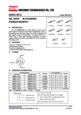
UNISONIC TECHNOLOGIES CO., LTD 8N65K-MTQ Power MOSFET 8A, 650V N-CHANNEL POWER MOSFET DESCRIPTION The UTC 8N65K-MTQ is a high voltage and high current power MOSFET designed to have better characteristics, such as fast switching time, low gate charge, low on-state resistance and high rugged avalanche characteristics. This power MOSFET is usually used in high speed switching... See More ⇒
8n65kl-ta3-t 8n65kg-ta3-t 8n65kl-tf3-t 8n65kg-tf3-t 8n65kl-tf1-t 8n65kg-tf1-t 8n65kl-tf2-t 8n65kg-tf2-t.pdf
UNISONIC TECHNOLOGIES CO., LTD 8N65K-MTQ Power MOSFET 8A, 650V N-CHANNEL POWER MOSFET DESCRIPTION The UTC 8N65K-MTQ is a high voltage and high current power MOSFET designed to have better characteristics, such as fast switching time, low gate charge, low on-state resistance and high rugged avalanche characteristics. This power MOSFET is usually used in high speed switching... See More ⇒
cjb08n65.pdf
JIANGSU CHANGJIANG ELECTRONICS TECHNOLOGY CO., LTD TO-263-2L Plastic-Encapsulate MOSFETS CJB08N65 N-Channel Power MOSFET TO-263-2L GENERAL DESCRIPTION This advanced high voltage MOSFET is designed to stand high energy in the avalanche mode and switch efficiently. This new high energy device also offers a drain-to-source diode fast recovery time. Desighed for high voltage, hig... See More ⇒
cjpf08n65.pdf
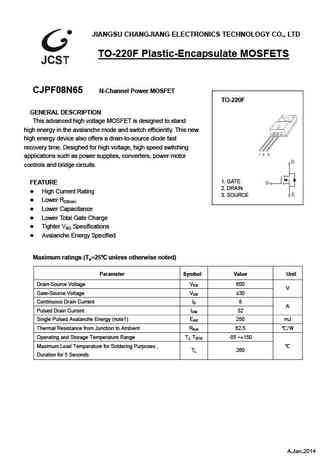
JIANGSU CHANGJIANG ELECTRONICS TECHNOLOGY CO., LTD TO-220F Plastic-Encapsulate MOSFETS CJPF08N65 N-Channel Power MOSFET TO-220F GENERAL DESCRIPTION This advanced high voltage MOSFET is designed to stand high energy in the avalanche mode and switch efficiently. This new high energy device also offers a drain-to-source diode fast recovery time. Desighed for high voltage, high s... See More ⇒
cjp08n65.pdf
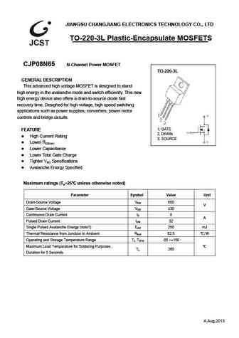
JIANGSU CHANGJIANG ELECTRONICS TECHNOLOGY CO., LTD TO-220-3L Plastic-Encapsulate MOSFETS CJP08N65 N-Channel Power MOSFET TO-220-3L GENERAL DESCRIPTION This advanced high voltage MOSFET is designed to stand high energy in the avalanche mode and switch efficiently. This new high energy device also offers a drain-to-source diode fast recovery time. Desighed for high voltage, hig... See More ⇒
kp8n65d.pdf
KP8N65D/I SEMICONDUCTOR N CHANNEL MOS FIELD TECHNICAL DATA EFFECT TRANSISTOR General Description KP8N65D This Super Junction MOSFET has better characteristics, such as fast switching time, low on resistance, low gate charge and excellent A K DIM MILLIMETERS L avalanche characteristics. It is mainly suitable for active power factor C D _ A 6.60 + 0.20 _ B 6.10 + 0.20 correctio... See More ⇒
aok18n65.pdf
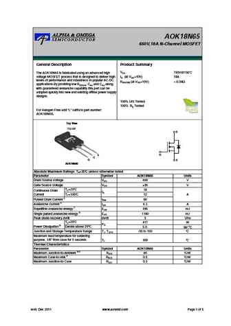
AOK18N65 650V,18A N-Channel MOSFET General Description Product Summary VDS 750V@150 The AOK18N65 is fabricated using an advanced high voltage MOSFET process that is designed to deliver high ID (at VGS=10V) 18A levels of performance and robustness in popular AC-DC RDS(ON) (at VGS=10V) ... See More ⇒
aotf18n65.pdf
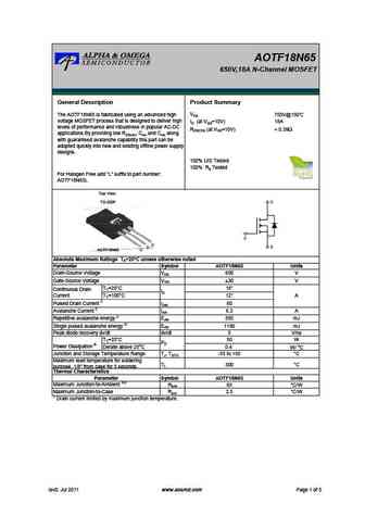
AOTF18N65 650V,18A N-Channel MOSFET General Description Product Summary VDS 750V@150 The AOTF18N65 is fabricated using an advanced high voltage MOSFET process that is designed to deliver high ID (at VGS=10V) 18A levels of performance and robustness in popular AC-DC RDS(ON) (at VGS=10V) ... See More ⇒
aot8n65 aotf8n65.pdf
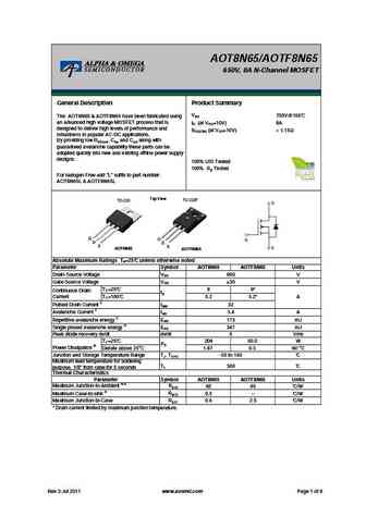
AOT8N65/AOTF8N65 650V, 8A N-Channel MOSFET General Description Product Summary VDS 750V@150 The AOT8N65 & AOTF8N65 have been fabricated using an advanced high voltage MOSFET process that is ID (at VGS=10V) 8A designed to deliver high levels of performance and RDS(ON) (at VGS=10V) ... See More ⇒
aotf18n65l.pdf
AOTF18N65 650V,18A N-Channel MOSFET General Description Product Summary VDS 750V@150 The AOTF18N65 is fabricated using an advanced high voltage MOSFET process that is designed to deliver high ID (at VGS=10V) 18A levels of performance and robustness in popular AC-DC RDS(ON) (at VGS=10V) ... See More ⇒
aok18n65l.pdf
AOK18N65 650V,18A N-Channel MOSFET General Description Product Summary VDS 750V@150 The AOK18N65 is fabricated using an advanced high voltage MOSFET process that is designed to deliver high ID (at VGS=10V) 18A levels of performance and robustness in popular AC-DC RDS(ON) (at VGS=10V) ... See More ⇒
aot8n65.pdf
AOT8N65/AOTF8N65 650V, 8A N-Channel MOSFET General Description Product Summary VDS 750V@150 The AOT8N65 & AOTF8N65 have been fabricated using an advanced high voltage MOSFET process that is ID (at VGS=10V) 8A designed to deliver high levels of performance and RDS(ON) (at VGS=10V) ... See More ⇒
aotf8n65.pdf
AOT8N65/AOTF8N65 650V, 8A N-Channel MOSFET General Description Product Summary VDS 750V@150 The AOT8N65 & AOTF8N65 have been fabricated using an advanced high voltage MOSFET process that is ID (at VGS=10V) 8A designed to deliver high levels of performance and RDS(ON) (at VGS=10V) ... See More ⇒
sif18n65c.pdf
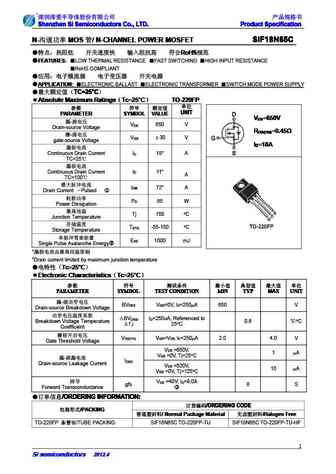
Shenzhen SI Semiconductors Co., LTD. Product Specification Shenzhen SI Semiconductors Co., LTD. Product Specification Shenzhen SI Semiconductors Co., LTD. Product Specification Shenzhen SI Semiconductors Co., LTD. Product Specification N- MOS / N-CHANNEL POWER MOSFET SIF18N65C N- MOS / N-CHANNEL POWER MOSFET SIF18N65C N- MOS / N-CHA... See More ⇒
jcs8n65v jcs8n65r jcs8n65c jcs8n65f jcs8n65s jcs8n65b.pdf
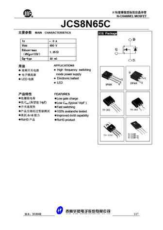
N R N-CHANNEL MOSFET JCS8N65C MAIN CHARACTERISTICS Package 8 8 8 8 8 8 8 8 8 ID .0 A VDSS 650 V Rdson-max 1.35 @Vgs=10V Qg-typ 32 nC APPLICATIONS High frequency switching mode power supply Electronic ballast LED ... See More ⇒
mtn8n65ea.pdf
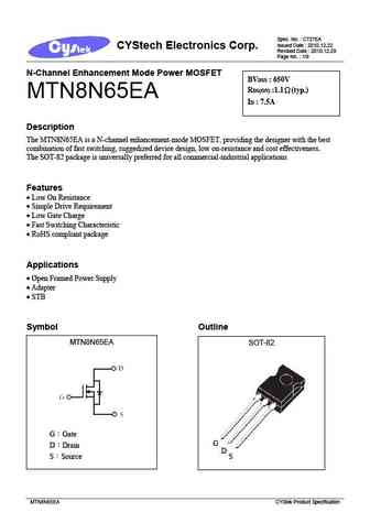
Spec. No. C727EA Issued Date 2010.12.22 CYStech Electronics Corp. Revised Date 2010.12.29 Page No. 1/9 N-Channel Enhancement Mode Power MOSFET BVDSS 650V RDS(ON) 1.1 (typ.) MTN8N65EA ID 7.5A Description The MTN8N65EA is a N-channel enhancement-mode MOSFET, providing the designer with the best combination of fast switching, ruggedized device design, low on-re... See More ⇒
mtn8n65e3.pdf
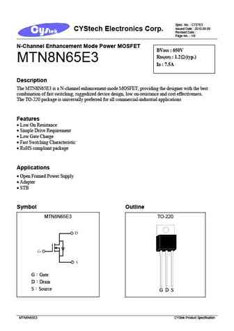
Spec. No. C727E3 Issued Date 2010.08.09 CYStech Electronics Corp. Revised Date Page No. 1/9 N-Channel Enhancement Mode Power MOSFET BVDSS 650V RDS(ON) 1.2 (typ.) MTN8N65E3 ID 7.5A Description The MTN8N65E3 is a N-channel enhancement-mode MOSFET, providing the designer with the best combination of fast switching, ruggedized device design, low on-resistance a... See More ⇒
mtn8n65fi.pdf
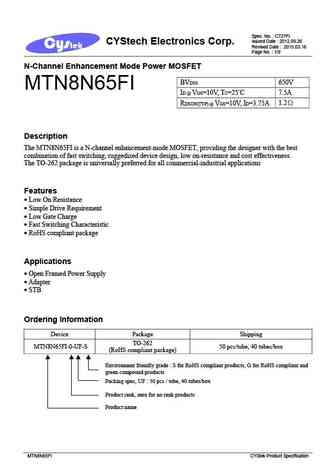
Spec. No. C727FI Issued Date 2012.09.26 CYStech Electronics Corp. Revised Date 2015.03.16 Page No. 1/9 N-Channel Enhancement Mode Power MOSFET BVDSS 650V MTN8N65FI ID @ VGS=10V, TC=25 C 7.5A 1.2 RDSON(TYP) @ VGS=10V, ID=3.75A Description The MTN8N65FI is a N-channel enhancement-mode MOSFET, providing the designer with the best combination of fast switching, r... See More ⇒
mtn8n65fp.pdf
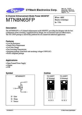
Spec. No. C727FP Issued Date 2009.06.23 CYStech Electronics Corp. Revised Date 2012.10.08 Page No. 1/11 N-Channel Enhancement Mode Power MOSFET BVDSS 650V RDS(ON) 1.2 (typ.) MTN8N65FP ID 7.5A Description The MTN8N65FP is a N-channel enhancement-mode MOSFET, providing the designer with the best combination of fast switching, ruggedized device design, low on-r... See More ⇒
ssf8n65.pdf
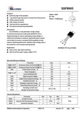
SSF8N65 Features VDSS = 650V Extremely high dv/dt capability ID = 8A Low Gate Charge Qg results in Simple Drive Requirement Rdson = 0.95 (typ.) 100% avalanche tested Gate charge minimized Very low intrinsic capacitances Very good manufacturing repeatability Description The SSF8N65 is a new generation of high voltage N Channel enhancement mod... See More ⇒
ita08n65r.pdf
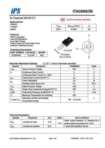
ITA08N65R N-Channel MOSFET Lead Free Package and Finish Applications Adaptor VDSS RDS(ON)(Typ.) ID Charger SMPS 650V 0.86 8A Features RoHS Compliant Low ON Resistance Low Gate Charge Peak Current vs Pulse Width Curve Inductive Switching Curves Ordering Information PART NUMBER PACKAGE BRAND ITA08N65R TO-220F IPS Absolute M... See More ⇒
brfl8n65.pdf
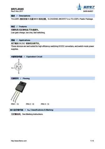
BRFL8N65 Rev.E Nov.-2017 DATA SHEET / Descriptions TO-220FL N MOS N-CHANNEL MOSFET in a TO-220FL Plastic Package. / Features , , Low gate charge, low crss, fast switching. / Applications DC/DC These devices are well suited for high efficien... See More ⇒
brf8n65.pdf
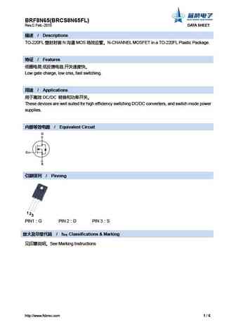
BRF8N65(BRCS8N65FL) Rev.C Feb.-2015 DATA SHEET / Descriptions TO-220FL N MOS N-CHANNEL MOSFET in a TO-220FL Plastic Package. / Features , , Low gate charge, low crss, fast switching. / Applications DC/DC These devices are well suited for hi... See More ⇒
cs8n65f a9h.pdf
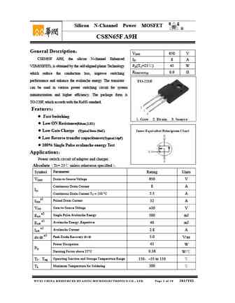
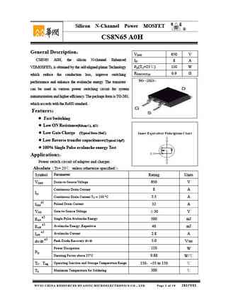
Silicon N-Channel Power MOSFET R CS8N65F A9H General Description VDSS 650 V CS8N65F A9H, the silicon N-channel Enhanced ID 8 A PD(TC=25 ) 45 W VDMOSFETs, is obtained by the self-aligned planar Technology RDS(ON)Typ 0.9 which reduce the conduction loss, improve switching performance and enhance the avalanche energy. The transistor can be used in various pow... See More ⇒
cs8n65 a0h.pdf
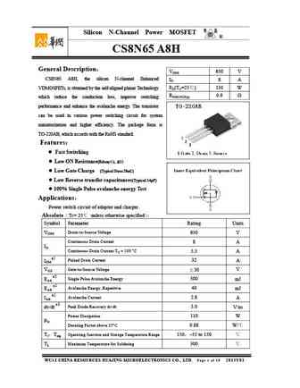
Silicon N-Channel Power MOSFET R CS8N65 A0H General Description VDSS 650 V CS8N65 A0H, the silicon N-channel Enhanced ID 8 A PD(TC=25 ) 110 W VDMOSFETs, is obtained by the self-aligned planar Technology RDS(ON)Typ 0.9 which reduce the conduction loss, improve switching performance and enhance the avalanche energy. The transistor can be used in various power... See More ⇒
cs8n65 a8h.pdf
Silicon N-Channel Power MOSFET R CS8N65 A8H General Description VDSS 650 V CS8N65 A8H, the silicon N-channel Enhanced ID 8 A VDMOSFETs, is obtained by the self-aligned planar Technology PD(TC=25 ) 110 W RDS(ON)Typ 0.9 which reduce the conduction loss, improve switching performance and enhance the avalanche energy. The transistor can be used in various power swi... See More ⇒
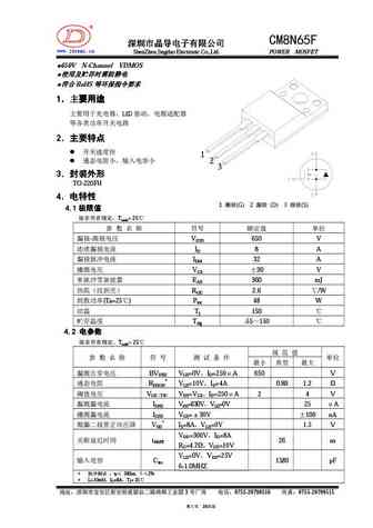
cm8n65f.pdf
R CM8N65F www.jdsemi.cn ShenZhen Jingdao Electronic Co.,Ltd. POWER MOSFET 650V N-Channel VDMOS RoHS ... See More ⇒
ftk8n65p f dd.pdf
SEMICONDUCTOR FTK8N65P / F / DD TECHNICAL DATA 8.0 Amps, 650 Volts N-CHANNEL MOSFET DESCRIPTION These N-Channel enhancement mode power field effect P Transistors are produced using planar stripe, DMOS technology. 1 This advanced technology has been especially tailored to minimize on - state resistance , provide superior TO-220 switching performance,and Withstand high energy pul... See More ⇒
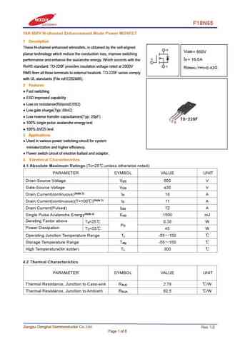
f18n65.pdf
F18N65 18A 650V N-channel Enhancement Mode Power MOSFET 1 Description These N-channel enhanced vdmosfets, is obtained by the self-aligned V DSS = 650V planar technology which reduce the conduction loss, improve switching I = 18.0A D performance and enhance the avalanche energy. Which accords with the RoHS standard. TO-220F provides insulation voltage rated at 2000V R DS(on) TYP) ... See More ⇒
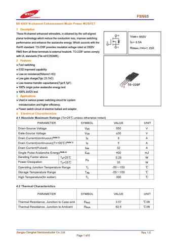
f8n65.pdf
F8N65 8A 650V N-channel Enhancement Mode Power MOSFET 1 Description These N-channel enhanced vdmosfets, is obtained by the self-aligned V DSS = 650V planar technology which reduce the conduction loss, improve switching I = 8.0A D performance and enhance the avalanche energy. Which accords with the RoHS standard. TO-220F provides insulation voltage rated at 2000V R DS(on) TYP) =1.... See More ⇒
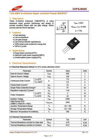
dhfsj8n65.pdf
DHFSJ8N65 7.6A 650V N-channel Super Junction Power MOSFET 1 Description These N-channel enhanced VDMOSFETs, is using 2 D V = 650V DSS advanced super junction technology and design to provide excellent Rdson with low gate charge. Which R = 0.48 DS(on) (TYP) G accords with the RoHS standard. 1 I = 7.6A 3 S D 2 Features Fast switching Low on resistance ... See More ⇒
svf8n65rmj svf8n65rdtr.pdf
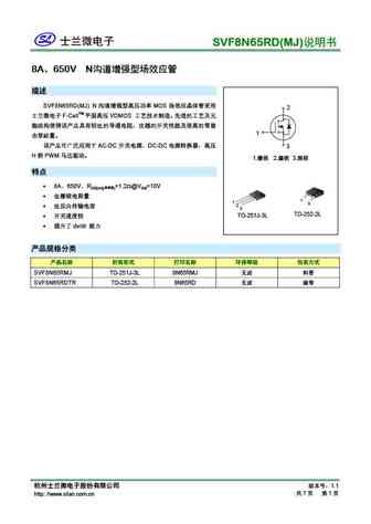
SVF8N65RD(MJ) 8A 650V N SVF8N65RD(MJ) N MOS 2 F-CellTM VDMOS 1 ... See More ⇒
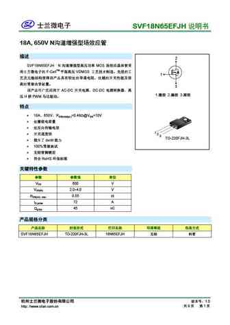
svf18n65f svf18n65t svf18n65pn.pdf
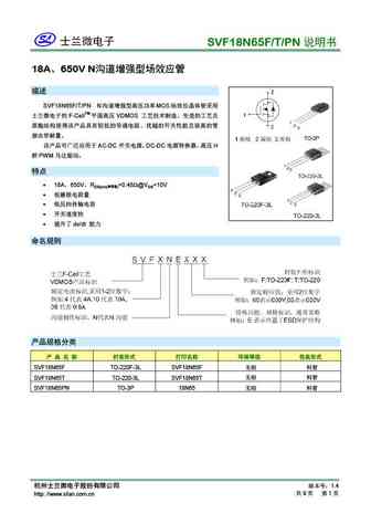
SVF18N65F/T/PN 18A 650V N SVF18N65F/T/PN N MOS F-CellTM VDMOS AC-DC ... See More ⇒
svf8n65t svf8n65f.pdf
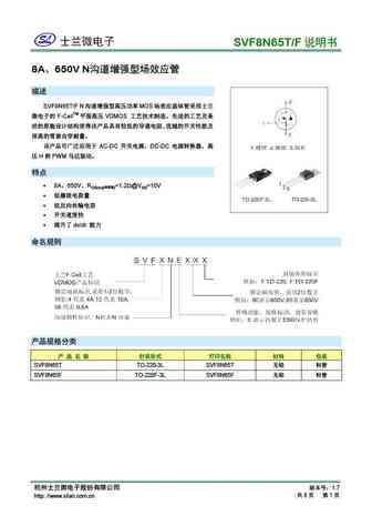
SVF8N65T/F 8A 650V N SVF8N65T/F N MOS F-CellTM VDMOS AC-D... See More ⇒
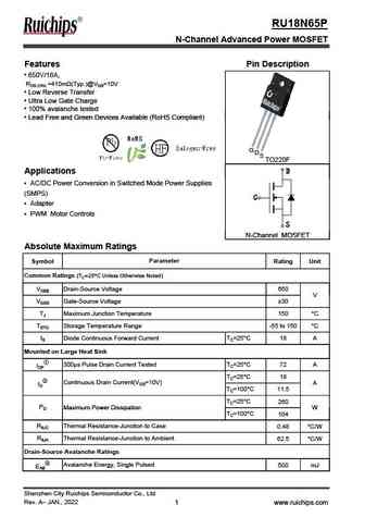
ru18n65p.pdf
RU18N65P N-Channel Advanced Power MOSFET Features Pin Description 650V/18A, RDS (ON) =410m (Typ.)@VGS=10V Low Reverse Transfer Ultra Low Gate Charge 100% avalanche tested Lead Free and Green Devices Available (RoHS Compliant) Lead Free and Green Devices Available (RoHS Compliant) GD S TO220F D D D D D Applications D pp D AC/DC Power Conversi... See More ⇒
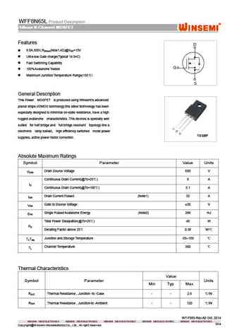
wff8n65l.pdf
WFF8N65L Product Description Silicon N-Channel MOSFET Silicon N-Channel MOSFET Silicon N-Channel MOSFET Silicon N-Channel MOSFET Features D 8.0A,650V,R (Max1.4 )@V =10V DS(on) GS Ultra-low Gate charge(Typical 14.5nC) Fast Switching Capability G 100%Avalanche Tested Maximum Junction Temperature Range(150 ) S General Description This Power MOSFET is produce... See More ⇒
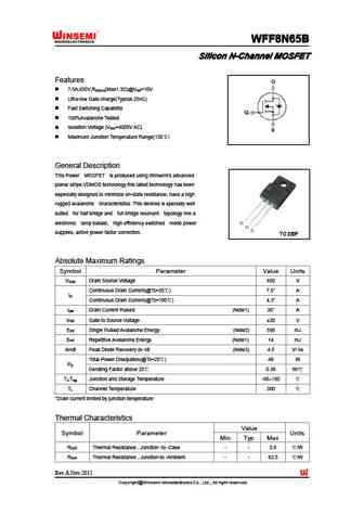
wff8n65b.pdf
WFF8N65B WFF8N65B WFF8N65B WFF8N65B Silicon N-Channel MOSFET Silicon N-Channel MOSFET Silicon N-Channel MOSFET Silicon N-Channel MOSFET Features 7.5A,650V,R (Max1.3 )@V =10V DS(on) GS Ultra-low Gate charge(Typical 25nC) Fast Switching Capability 100%Avalanche Tested Isolation Voltage (V =4000V AC) ISO Maximum Junction Temperature Range(150 ) General ... See More ⇒
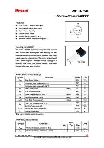
wfj8n65b.pdf
WFJ8N65B Silicon N-Channel MOSFET Features 7.5A,650V,R (Max1.3 )@V =10V DS(on) GS Ultra-low Gate charge(Typical 25nC) Fast Switching Capability 100%Avalanche Tested Isolation Voltage (V =4000V AC) ISO Maximum Junction Temperature Range(150 ) General Description This Power MOSFET is produced using Winsemi's advanced planar stripe, VDMOS technology. this late... See More ⇒
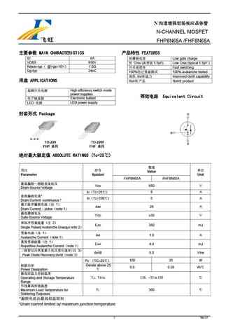
fhp8n65a fhf8n65a.pdf
N N-CHANNEL MOSFET FHP8N65A /FHF8N65A MAIN CHARACTERISTICS FEATURES ID 8A Low gate charge VDSS 650V Crss ( 5.5pF) Low Crss (typical 5.5pF ) Rdson-typ @Vgs=10V 1.0 Fast switching Qg-typ 24nC 100% 100% avalanche tested dv/dt Impr... See More ⇒
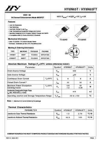
hy8n65t.pdf
HY8N65T / HY8N65FT 650V / 8A 650V, RDS(ON)=1.4 @VGS=10V, ID=4.0A N-Channel Enhancement Mode MOSFET Features Low ON Resistance Fast Switching Low Gate Charge & Low CRSS Fully Characterized Avalanche Voltage and Current Specially Desigened for AC Adapter, Battery Charger and SMPS 1 1 2 2 In compliance with EU RoHs 2002/95/EC Directives G G 3 3 D D S S ... See More ⇒
jfpc8n65c.pdf
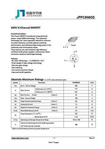
JFPC8N65C 650V N-Channel MOSFET General Description This Power MOSFET is produced using advanced planar stripe DMOS technology. This advanced technology has been especially tailored to minimize on-state resistance, provide superior switching performance, and withstand high energy pulse in the avalanche and commutation mode. These devices are well suited for high efficiency s... See More ⇒
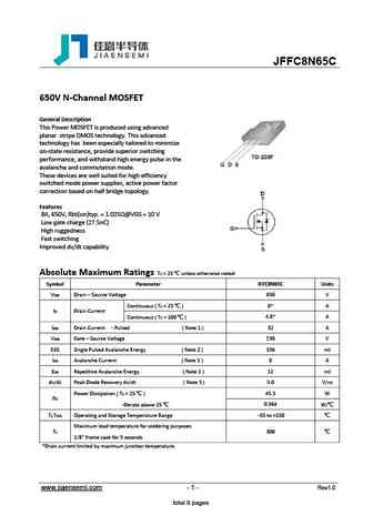
jffc8n65c.pdf
JFFC8N65C 650V N-Channel MOSFET General Description This Power MOSFET is produced using advanced planar stripe DMOS technology. This advanced technology has been especially tailored to minimize on-state resistance, provide superior switching performance, and withstand high energy pulse in the avalanche and commutation mode. These devices are well suited for high efficiency s... See More ⇒
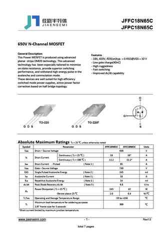
jfpc18n65c jffc18n65c.pdf
JFFC18N65C JFPC18N65C 650V N-Channel MOSFET General Description Features This Power MOSFET is produced using advanced - 18A, 650V, RDS(on)typ. = 0.45 @VGS = 10 V planar stripe DMOS technology. This advanced - Low gate charge(40nC) technology has been especially tailored to minimize - High ruggedness on-state resistance, provide superior switching - Fast switching perf... See More ⇒
jfpc8n65d.pdf
JFPC8N65D 650V N-Channel MOSFET General Description This Power MOSFET is produced using advanced planar stripe DMOS technology. This advanced technology has been especially tailored to minimize on-state resistance, provide superior switching performance, and withstand high energy pulse in the avalanche and commutation mode. These devices are well suited for high efficiency s... See More ⇒
jfpc18n65ci.pdf
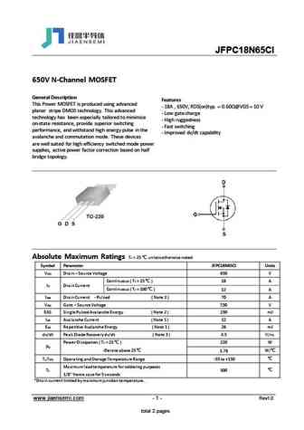
JFPC18N65CI 650V N-Channel MOSFET General Description Features This Power MOSFET is produced using advanced - 18A , 650V, RDS(on)typ. = 0.60 @VGS = 10 V planar stripe DMOS technology. This advanced - Low gate charge technology has been especially tailored to minimize - High ruggedness on-state resistance, provide superior switching - Fast switching performance, and wit... See More ⇒
slp8n65c slf8n65c.pdf
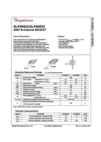
SLP8N65C/SLF8N65C 650V N-Channel MOSFET General Description Features This Power MOSFET is produced using Maple semi s - 7.5A, 650V, RDS(on) typ. = 1.2 @VGS = 10 V advanced planar stripe DMOS technology. - Low gate charge ( typical 29nC) This advanced technology has been especially tailored - High ruggedness to minimize on-state resistance, provide superior switching - Fast switching p... See More ⇒
ptp08n65 pta08n65.pdf
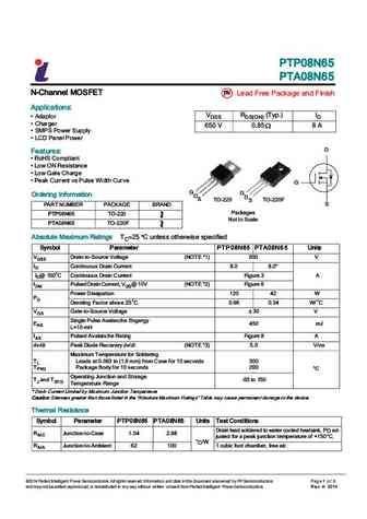
PTP08N65 PTA08N65 N-Channel MOSFET Pb Lead Free Package and Finish Applications VDSS RDS(ON) (Typ.) ID Adaptor Charger 650 V 0.85 8 A SMPS Power Supply LCD Panel Power D Features RoHS Compliant Low ON Resistance Low Gate Charge Peak Current vs Pulse Width Curve G G G Ordering Information DS DS TO-220F TO-220 S PART NUMBER PACKAGE... See More ⇒
swt38n65k2.pdf
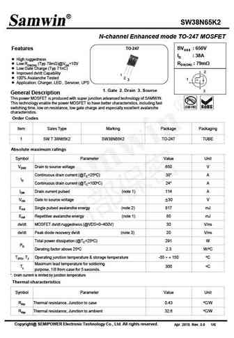
SW38N65K2 N-channel Enhanced mode TO-247 MOSFET TO-247 BVDSS 650V Features ID 38A High ruggedness RDS(ON) 79m Low RDS(ON) (Typ 79m )@VGS=10V Low Gate Charge (Typ 71nC) 2 Improved dv/dt Capability 1 100% Avalanche Tested 2 1 3 Application Charger, LED , Servicer, UPS 1. Gate 2. Drain 3. Source 3 General Description This ... See More ⇒
swu8n65k.pdf
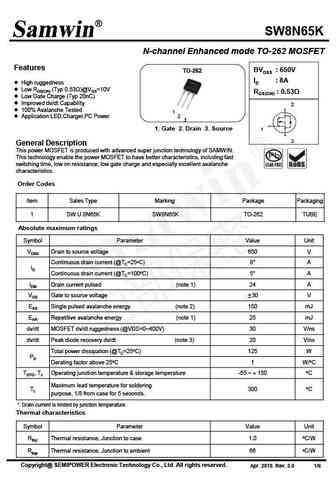
SW8N65K N-channel Enhanced mode TO-262 MOSFET Features BVDSS 650V TO-262 ID 8A High ruggedness Low RDS(ON) (Typ 0.53 )@VGS=10V RDS(ON) 0.53 Low Gate Charge (Typ 20nC) Improved dv/dt Capability 2 100% Avalanche Tested 1 Application LED,Charger,PC Power 2 3 1. Gate 2. Drain 3. Source 1 3 General Description This power MOS... See More ⇒
swp8n65d swi8n65d swd8n65d swf8n65d swnx8n65d.pdf
SW8N65D N-channel Enhanced mode TO-220/TO-251/TO-252/TO-220F/TO-251NX MOSFET BVDSS 650V Features TO-220 TO-251 TO-252 TO-220F TO-251NX ID 8A High ruggedness RDS(ON) 1.1 Low RDS(ON) (Typ 1.1 )@VGS=10V Low Gate Charge (Typ 32nC) 2 Improved dv/dt Capability 1 1 1 1 100% Avalanche Tested 1 2 2 2 2 2 3 3 3 3 Application Charg... See More ⇒
swt38n65k.pdf
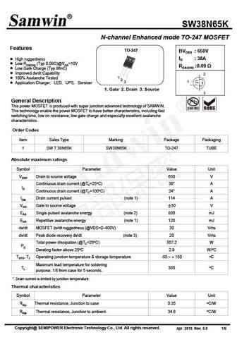
SW38N65K N-channel Enhanced mode TO-247 MOSFET Features TO-247 BVDSS 650V ID 38A High ruggedness Low RDS(ON) (Typ 0.09 )@VGS=10V RDS(ON) 0.09 Low Gate Charge (Typ 96nC) Improved dv/dt Capability 2 1 100% Avalanche Tested 2 1 3 Application Charger LED UPS Servicer 1. Gate 2. Drain 3. Source 3 General Description ... See More ⇒
swt38n65k2f swx38n65k2f.pdf
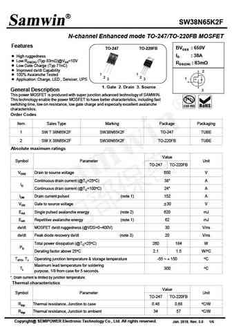
SW38N65K2F N-channel Enhanced mode TO-247/TO-220FB MOSFET Features TO-247 TO-220FB BVDSS 650V ID 38A High ruggedness Low RDS(ON) (Typ 83m )@VGS=10V RDS(ON) 83m Low Gate Charge (Typ 71nC) Improved dv/dt Capability 2 1 1 100% Avalanche Tested 2 2 1 3 3 Application Charge, LED , Servicer, UPS 1. Gate 2. Drain 3. Source Gener... See More ⇒
swmn8n65la.pdf
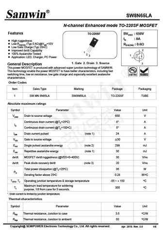
SW8N65LA N-channel Enhanced mode TO-220SF MOSFET Features TO-220SF BVDSS 650V ID 8A High ruggedness Low RDS(ON) (Typ 0.6 )@VGS=10V RDS(ON) 0.6 Low Gate Charge (Typ 20nC) 2 Improved dv/dt Capability 1 100% Avalanche Tested 2 1 3 Application LED, Charger, PC Power 1. Gate 2. Drain 3. Source 3 General Description This po... See More ⇒
sw38n65kf swt38n65kf.pdf
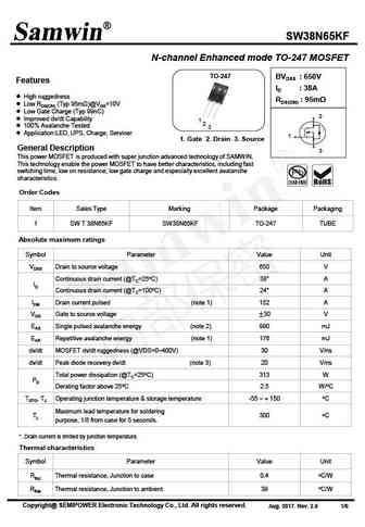
SW38N65KF N-channel Enhanced mode TO-247 MOSFET TO-247 BVDSS 650V Features ID 38A High ruggedness RDS(ON) 95m Low RDS(ON) (Typ 95m )@VGS=10V Low Gate Charge (Typ 99nC) 2 Improved dv/dt Capability 1 2 100% Avalanche Tested 3 Application LED, UPS, Charge, Servicer 1 1. Gate 2. Drain 3. Source General Description 3 This p... See More ⇒
sw8n65db swi8n65db swd8n65db swf8n65db swj8n65db.pdf
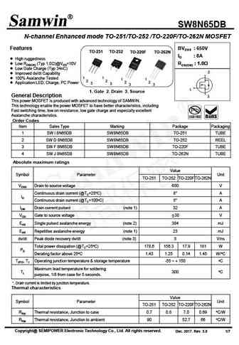
SW8N65DB N-channel Enhanced mode TO-251/TO-252 /TO-220F/TO-262N MOSFET Features BVDSS 650V TO-251 TO-252 TO-220F TO-262N ID 8A High ruggedness Low RDS(ON) (Typ 1.0 )@VGS=10V RDS(ON) 1.0 Low Gate Charge (Typ 34nC) 2 Improved dv/dt Capability 1 100% Avalanche Tested 1 1 1 2 2 2 2 Application LED, Charge, PC Power 3 3 3 3 1... See More ⇒
swf18n65d swt18n65d.pdf
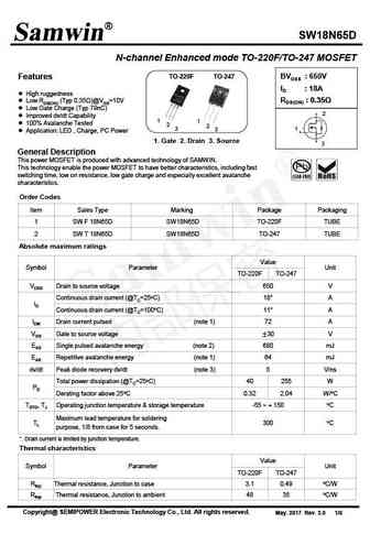
SW18N65D N-channel Enhanced mode TO-220F/TO-247 MOSFET TO-220F TO-247 BVDSS 650V Features ID 18A High ruggedness RDS(ON) 0.35 Low RDS(ON) (Typ 0.35 )@VGS=10V Low Gate Charge (Typ 79nC) 2 Improved dv/dt Capability 1 1 100% Avalanche Tested 2 2 3 1 3 Application LED , Charger, PC Power 1. Gate 2. Drain 3. Source 3 Gen... See More ⇒
sw18n65d swf18n65d swt18n65d.pdf
SW18N65D N-channel Enhanced mode TO-220F/TO-247 MOSFET TO-220F TO-247 BVDSS 650V Features ID 18A High ruggedness RDS(ON) 0.35 Low RDS(ON) (Typ 0.35 )@VGS=10V Low Gate Charge (Typ 79nC) 2 Improved dv/dt Capability 1 1 100% Avalanche Tested 2 2 3 1 3 Application LED , Charge, PC Power 1. Gate 2. Drain 3. Source 3 Gene... See More ⇒
swt38n65kf.pdf
SW38N65KF N-channel Enhanced mode TO-247 MOSFET TO-247 BVDSS 650V Features ID 38A High ruggedness RDS(ON) 95m Low RDS(ON) (Typ 95m )@VGS=10V Low Gate Charge (Typ 99nC) 2 Improved dv/dt Capability 1 2 100% Avalanche Tested 3 Application LED, UPS, Charger, Servicer 1 1. Gate 2. Drain 3. Source General Description 3 This ... See More ⇒
swi8n65db swd8n65db swf8n65db swj8n65db.pdf
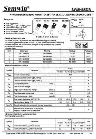
SW8N65DB N-channel Enhanced mode TO-251/TO-252 /TO-220F/TO-262N MOSFET Features BVDSS 650V TO-251 TO-252 TO-220F TO-262N ID 8A High ruggedness Low RDS(ON) (Typ 1.0 )@VGS=10V RDS(ON) 1.0 Low Gate Charge (Typ 34nC) 2 Improved dv/dt Capability 1 100% Avalanche Tested 1 1 1 2 2 2 2 Application LED, Charger, PC Power 3 3 3 3 1 1. Gate 2. Drain ... See More ⇒
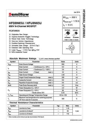
hfd8n65u.pdf
Jan 2014 BVDSS = 650 V RDS(on) typ HFD8N65U / HFU8N65U ID = 6.0 A 650V N-Channel MOSFET D-PAK I-PAK FEATURES 2 1 Originative New Design 1 3 2 3 Superior Avalanche Rugged Technology HFD8N65U HFU8N65U Robust Gate Oxide Technology 1.Gate 2. Drain 3. Source Very Low Intrinsic Capacitances Excellent Switching Characteristics Unrivalled Gate Charge 22.0 n... See More ⇒
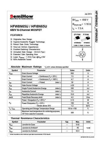
hfw8n65u.pdf
Jan 2013 BVDSS = 650 V RDS(on) typ HFW8N65U / HFI8N65U ID = 7.5 A 650V N-Channel MOSFET D2-PAK I2-PAK FEATURES Originative New Design Superior Avalanche Rugged Technology HFW8N65U HFI8N65U Robust Gate Oxide Technology 1.Gate 2. Drain 3. Source Very Low Intrinsic Capacitances Excellent Switching Characteristics Unrivalled Gate Charge 22.0 nC (Typ.) Ext... See More ⇒
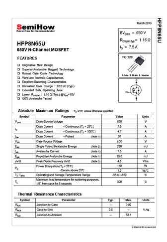
hfp8n65u.pdf
March 2013 BVDSS = 650 V RDS(on) typ HFP8N65U ID = 7.5 A 650V N-Channel MOSFET TO-220 FEATURES Originative New Design Superior Avalanche Rugged Technology 1 2 3 Robust Gate Oxide Technology 1.Gate 2. Drain 3. Source Very Low Intrinsic Capacitances Excellent Switching Characteristics Unrivalled Gate Charge 22.0 nC (Typ.) Extended Safe Operating Area ... See More ⇒
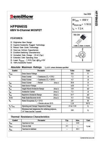
hfp8n65s.pdf
Sep 2009 BVDSS = 650 V RDS(on) typ HFP8N65S ID = 7.2 A 650V N-Channel MOSFET TO-220 FEATURES Originative New Design 1 2 3 Superior Avalanche Rugged Technology 1.Gate 2. Drain 3. Source Robust Gate Oxide Technology Very Low Intrinsic Capacitances Excellent Switching Characteristics Unrivalled Gate Charge 22 nC (Typ.) Extended Safe Operating Area Lower RDS(O... See More ⇒
hfs8n65u.pdf
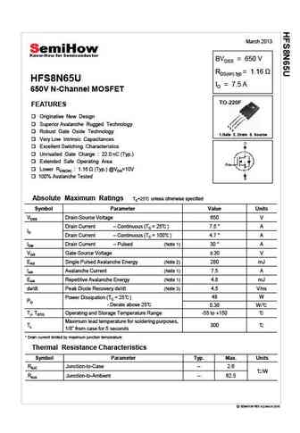
March 2013 BVDSS = 650 V RDS(on) typ HFS8N65U ID = 7.5 A 650V N-Channel MOSFET TO-220F FEATURES Originative New Design Superior Avalanche Rugged Technology 1 2 3 Robust Gate Oxide Technology 1.Gate 2. Drain 3. Source Very Low Intrinsic Capacitances Excellent Switching Characteristics Unrivalled Gate Charge 22.0 nC (Typ.) Extended Safe Operating Area... See More ⇒
hfs8n65s.pdf
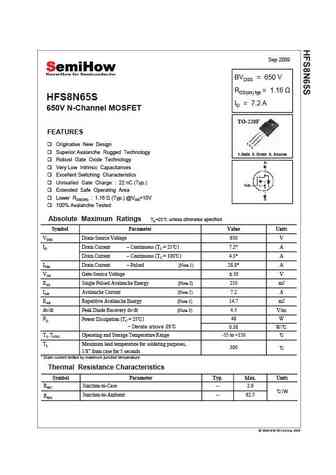
Sep 2009 BVDSS = 650 V RDS(on) typ = 1.16 HFS8N65S ID = 7.2 A 650V N-Channel MOSFET TO-220F FEATURES 1 Originative New Design 2 3 Superior Avalanche Rugged Technology 1.Gate 2. Drain 3. Source Robust Gate Oxide Technology Very Low Intrinsic Capacitances Excellent Switching Characteristics Unrivalled Gate Charge 22 nC (Typ.) Unrivalled Gate Charge 22 nC (Typ ) E... See More ⇒
hfs8n65sa.pdf
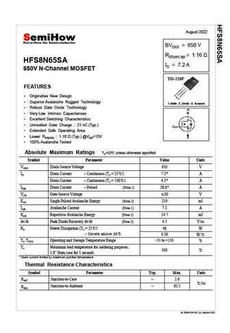
August 2022 BVDSS = 650 V RDS(on) typ = 1.16 HFS8N65SA ID = 7.2 A 650V N-Channel MOSFET TO-220F FEATURES 1 Originative New Design 2 3 Superior Avalanche Rugged Technology 1.Gate 2. Drain 3. Source Robust Gate Oxide Technology Very Low Intrinsic Capacitances Excellent Switching Characteristics Unrivalled Gate Charge 21 nC (Typ.) Extended Safe O... See More ⇒
hfs8n65js.pdf
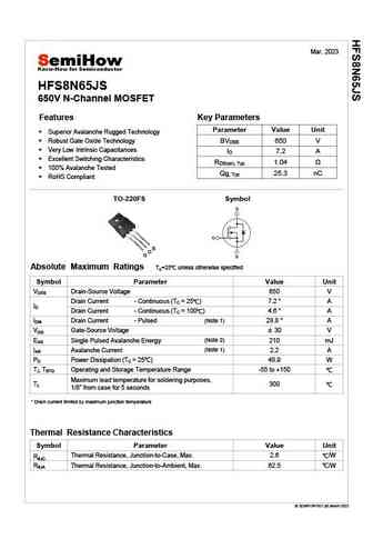
Mar. 2023 HFS8N65JS 650V N-Channel MOSFET Features Key Parameters Parameter Value Unit Superior Avalanche Rugged Technology BVDSS 650 V Robust Gate Oxide Technology Very Low Intrinsic Capacitances ID 7.2 A Excellent Switching Characteristics RDS(on), Typ 1.04 100% Avalanche Tested Qg, Typ 25.3 nC RoHS Compliant TO-220FS Symbol S D G Absolute Maximum... See More ⇒
tsp8n65m tsf8n65m.pdf
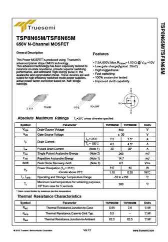
TSP8N65M/TSF8N65M 650V N-Channel MOSFET General Description Features This Power MOSFET is produced using Truesemi s 7.5A,650V,Max.RDS(on)=1.50 @ VGS =10V advanced planar stripe DMOS technology. This advanced technology has been especially tailored to Low gate charge(typical 29nC) minimize on-state resistance, provide superior switching High ruggedness performance, an... See More ⇒
wml28n65f2 wmk28n65f2 wmn28n65f2 wmm28n65f2 wmj28n65f2.pdf
WML28N65F2, WM F2 MK28N65F WMN2 N65F2, WM F2 28N65F2, WMM28N MJ28N65F 650V 0.15 S T V Super Junction Power MOSFET Descrip ption WMOSTM F2 is Wa 2nd generation super ayon s junction MOSFET fam with fa body di F2 M mily ast iode. S series pro all benefits of a fast switching ovide b f s S D D G G G S D G SJ-MOSFE while of an extremely fa body ET fferin... See More ⇒
wml08n65em wmk08n65em wmm08n65em wmn08n65em wmp08n65em wmo08n65em.pdf
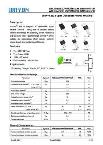
WML08 WMK08N6 8N65EM, W 65EM, WMM08N65EM WMN08 WMP08N6 8N65EM, W 65EM, WMO08N65EM 650V 0.8 S unction Power M T V Super Ju MOSFET Descrip ption WMOSTM EM is Wayon s 3rd generation super W n junction MOSFET fa that is utilizing charge M amily S balance te or extremely esistance echnology fo y low on-re S D D G G G S D G T and low ga ce. WMOSTM EM is a... See More ⇒
wml28n65c4 wmk28n65c4 wmn28n65c4 wmm28n65c4 wmj28n65c4.pdf
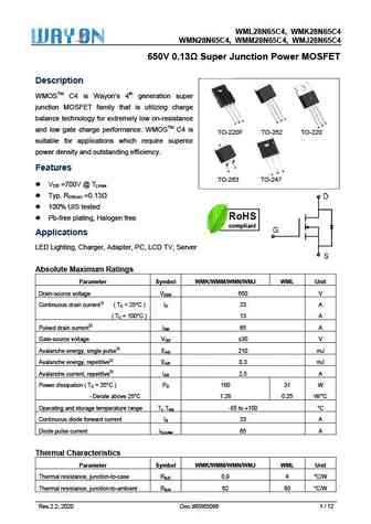
WML28N6 WM C4 65C4, MK28N65C WMN2 MJ28N65C 28N65C4, WMM28N65C4, WM C4 650V 0.13 S T V Super Junction Power MOSFET Descrip ption WMOSTM C4 is Wa 4th generation super ayon s n junction MOSFET fa that is utilizing charge M amily S balance te or extremely esistance echnology fo y low on-re S D D G G G S D G and low ga charge performanc WMOSTM C4 is ate c... See More ⇒
wml18n65em wmk18n65em wmm18n65em wmn18n65em wmp18n65em wmo18n65em.pdf
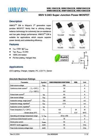
WML18 WMK18N6 8N65EM, W 65EM, WMM18N65EM WMN18 WMP18N6 8N65EM, W 65EM, WMO18N65EM 650V Super Ju MOSFET V 0.24 S unction Power M T Descrip ption WMOSTM EM is Wayon s 3rd generation super W n junction MOSFET fa that is utilizing charge M amily S balance te or extremely esistance echnology fo y low on-re S D D G G G S D G T and low ga ce. WMOSTM EM is ... See More ⇒
wmm08n65c4 wml08n65c4 wmo08n65c4 wmn08n65c4 wmp08n65c4 wmk08n65c4.pdf
WMM0 65C4, MO08N65C 08N65C4, WML08N6 WM C4 WMN0 65C4, MK08N65C 08N65C4, WMP08N6 WM C4 650V 0.65 S unction Power M T Super Ju MOSFET Descrip ption WMOSTM C4 is Wa 4th generation super ayon s n junction MOSFET fa that is utilizing charge M amily S balance te or extremely esistance echnology fo y low on-re D S D G G G S D G and low ga charge performanc ... See More ⇒
cs8n65a0h.pdf
Silicon N-Channel Power MOSFET R CS8N65 A0H General Description VDSS 650 V CS8N65 A0H, the silicon N-channel Enhanced ID 8 A PD(TC=25 ) 110 W VDMOSFETs, is obtained by the self-aligned planar Technology RDS(ON)Typ 0.9 which reduce the conduction loss, improve switching performance and enhance the avalanche energy. The transistor can be used in various power... See More ⇒
cs8n65a8h.pdf
Silicon N-Channel Power MOSFET R CS8N65 A8H General Description VDSS 650 V CS8N65 A8H, the silicon N-channel Enhanced ID 8 A VDMOSFETs, is obtained by the self-aligned planar Technology PD(TC=25 ) 110 W RDS(ON)Typ 0.9 which reduce the conduction loss, improve switching performance and enhance the avalanche energy. The transistor can be used in various power swi... See More ⇒
cs8n65fa9h.pdf
Silicon N-Channel Power MOSFET R CS8N65F A9H General Description VDSS 650 V CS8N65F A9H, the silicon N-channel Enhanced ID 8 A PD(TC=25 ) 45 W VDMOSFETs, is obtained by the self-aligned planar Technology RDS(ON)Typ 0.9 which reduce the conduction loss, improve switching performance and enhance the avalanche energy. The transistor can be used in various pow... See More ⇒
cs8n65f cs8n65p cs8n65d cs8n65f-b.pdf
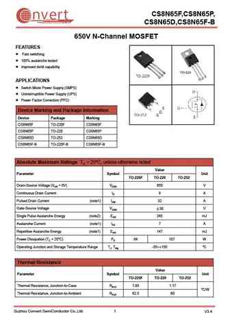
CS8N65F,CS8N65P, nvert Suzhou Convert Semiconductor Co ., Ltd. CS8N65D,CS8N65F-B 650V N-Channel MOSFET FEATURES Fast switching 100% avalanche tested Improved dv/dt capability APPLICATIONS Switch Mode Power Supply (SMPS) Uninterruptible Power Supply (UPS) Power Factor Correction (PFC) Device Marking and Package Information Device Package Marking CS8N65F TO... See More ⇒
cs8n60f cs8n60p cs8n60u cs8n60d cs8n65f-b.pdf
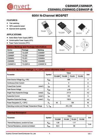
CS8N60F,CS8N60P, nvert Suzhou Convert Semiconductor Co ., Ltd. CS8N60U,CS8N60D,CS8N65F-B 600V N-Channel MOSFET FEATURES Fast switching 100% avalanche tested Improved dv/dt capability APPLICATIONS Switch Mode Power Supply (SMPS) Uninterruptible Power Supply (UPS) Power Factor Correction (PFC) Device Marking and Package Information Device Package Marking CS... See More ⇒
cs8n65f cs8n65p.pdf
nvert Suzhou Convert Semiconductor Co ., Ltd. CS8N65F,CS8N65P 650V N-Channel MOSFET FEATURES Fast switching 100% avalanche tested Improved dv/dt capability APPLICATIONS Switch Mode Power Supply (SMPS) Uninterruptible Power Supply (UPS) Power Factor Correction (PFC) Device Marking and Package Information Device Package Marking CS8N65F TO-220F CS8N65F CS8N65P... See More ⇒
fir8n65fg.pdf
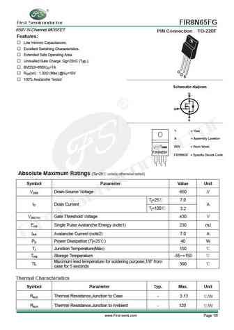
FIR8N65FG 650V N-Channel MOSFET PIN Connection TO-220F Features Low Intrinsic Capacitances. Excellent Switching Characteristics. Extended Safe Operating Area. Unrivalled Gate Charge Qg=28nC (Typ.). BVDSS=650V,ID=7A G RDS(on) 1.30 (Max) @VG=10V D S 100% Avalanche Tested g Schematic dia ram D G S Y = Year A = Assembly Location WW = W... See More ⇒
fir18n65fg.pdf
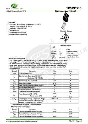
FIR18N65FG 650V N-Channel MOSFET-D . PIN Connection TO-220F Features 18A, 650V, RDS(on) = 380m @VGS = 10 V Low gate charge ( typical 38nC) G D S Low Crss ( typical 6.2pF) Fast switching Schematic diagram 100% avalanche tested D Improved dv/dt capability G S Marking Diagram Y = Year A = Assembly Location YAWWVT WW = Work Week FIR18N65F VT = ... See More ⇒
smf8n65.pdf
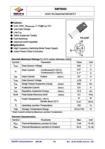
SMF8N65 650V N-Channnel MOSFET Features 8.0A, 650V, R =1.1 @V =10V DS(on)(Typ) GS Low Gate Charge Low C rss 100% Avalanche Tested Fast Switching Improved dv/dt Capability Application High Frequency Switching Mode Power Supply Active Power Factor Correction Absolute Maximum Ratings(Tc=25 C unless otherwise noted) Symbol Parameter Value... See More ⇒
ptf8n65.pdf
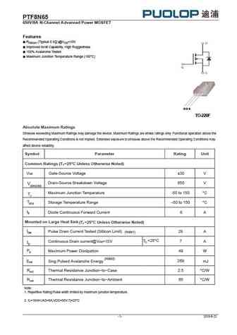
PTF8 N65 65 0V/8 A N-Channel A dv anced Power MOSFET Features RDS(on) (Typical 0.9 )@VGS=10V Improved dv/dt Capability, High Ruggedness 100% Avalanche Tested Maximum Junction Temperature Range (150 C) G D S TO-220F Absolute Maximum Ratings Stresses exceeding Maximum Ratings may damage the device. Maximum Ratings are stress ratings only. Functional operation above t... See More ⇒
se8n65a.pdf
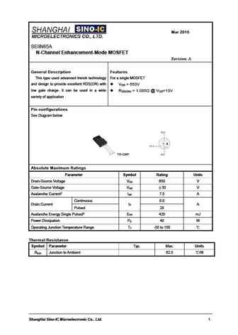
Mar 2015 SE8N65A N-Channel Enhancement-Mode MOSFET Revision A General Description Features This type used advanced trench technology For a single MOSFET and design to provide excellent RDS(ON) with V = 650V DS low gate charge. It can be used in a wide R = 1.085 @ V =10V DS(ON) GS variety of application Pin configurations See Diagram below TO-220F Absolute Maximum Rati... See More ⇒
smirf8n65.pdf
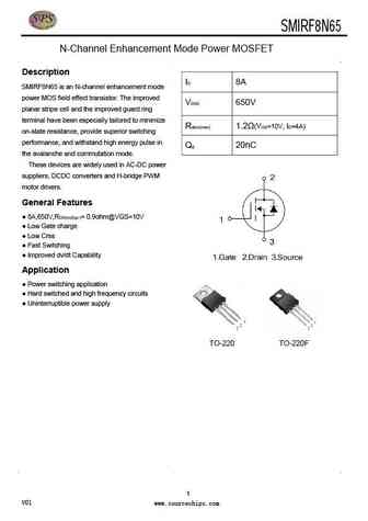
SMIRF8N65 30V /36A Single N Power MOSFET N-Channel Enhancement Mode Power MOSFET Description ID 8A SMIRF8N65 is an N-channel enhancement mode power MOS field effect transistor. The improved VDSS 650V planar stripe cell and the improved guard ring terminal have been especially tailored to minimize Rdson(max) 1.2 (VGS=10V, ID=4A) on-state resistance, provide superior switchi... See More ⇒
vbzmb18n65.pdf
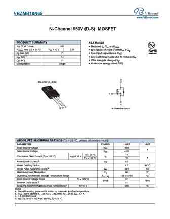
VBZMB18N65 www.VBsemi.com N-Channel 650V (D-S) MOSFET PRODUCT SUMMARY FEATURES VDS (V) at TJ max. 650 Reduced trr, Qrr, and IRRM RDS(on) max. ( ) at 25 C VGS = 10 V 0.50 Low figure-of-merit (FOM) Ron x Qg Qg max. (nC) Low input capacitance (Ciss) 71 Qgs (nC) 14 Low switching losses due to reduced Qrr Ultra low gate charge (Qg) Qgd (nC) 33 Avalanche ener... See More ⇒
tma8n65h tmc8n65h tmd8n65h tmu8n65h.pdf
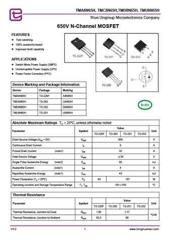
TMA8N65H, TMC8N65H,TMD8N65H, TMU8N65H Wuxi Unigroup Microelectronics Company 650V N-Channel MOSFET FEATURES Fast switching 100% avalanche tested Improved dv/dt capability APPLICATIONS Switch Mode Power Supply (SMPS) Uninterruptible Power Supply (UPS) Power Factor Correction (PFC) Device Marking and Package Information Device Package Marking TMA... See More ⇒
hms8n65 hms8n65f hms8n65d.pdf
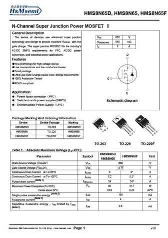
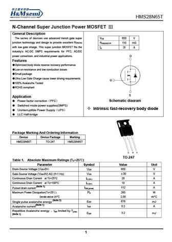
HMS8N65D, HMS8N65, HMS8N65F N-Channel Super Junction Power MOSFET General Description The series of devices use advanced super junction VDS 650 V technology and design to provide excellent RDS(ON) with low RDS(ON) MAX 540 m gate charge. This super junction MOSFET fits the industry s ID 8 A AC-DC SMPS requirements for PFC, AC/DC power conversion, and industrial power applic... See More ⇒
hms8n65k hms8n65i.pdf
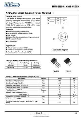
HMS8N65I, HMS8N65K N-Channel Super Junction Power MOSFET General Description The series of devices use advanced super junction VDS 650 V technology and design to provide excellent RDS(ON) with low RDS(ON) MAX 540 m gate charge. This super junction MOSFET fits the industry s ID 8 A AC-DC SMPS requirements for PFC, AC/DC power conversion, and industrial power applications. ... See More ⇒
hms28n65 hms28n65d hms28n65f.pdf
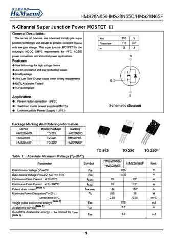
HMS28N65/HMS28N65D/HMS28N65F N-Channel Super Junction Power MOSFET General Description The series of devices use advanced trench gate super V 650 V DS junction technology and design to provide excellent RDS(ON) R 110 m DS(ON)TYP with low gate charge. This super junction MOSFET fits the ID 28 A industry s AC-DC SMPS requirements for PFC, AC/DC power conversion, and ind... See More ⇒
hms28n65t.pdf
HMS28N65T N-Channel Super Junction Power MOSFET General Description The series of devices use advanced trench gate super V 650 V DS junction technology and design to provide excellent RDS(ON) R 110 m DS(ON)TYP with low gate charge. This super junction MOSFET fits the ID 28 A industry s AC-DC SMPS requirements for PFC, AC/DC power conversion, and industrial power appli... See More ⇒
mpf8n65.pdf
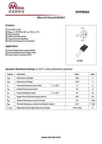
Silicon N-Channel MOSFET Features V =650V, I =8A DS D R = 1.4 (Max.) @ V = 10V, I = 4A DS(ON) GS D Fast switching 100% avalanche tested Improved dv/dt capability RoHS and Halogen-Free Compliant Application Switch Mode Power Supply (SMPS) Uninterruptible Power Supply (UPS) Power Factor Correction (PFC) TO-220 Absolute Maximum Ratings T =25 ... See More ⇒
fxn8n65d.pdf
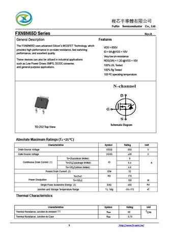
FuXin Semiconductor Co., Ltd. FXN8N65D Series Rev.A General Description Features The FXN8N65D uses advanced Silicon s MOSFET Technology, which VDS = 650V provides high performance in on-state resistance, fast switching ID = 8A @VGS = 10V performance, and excellent quality. Very low on-resistance These devices can also be utilized in industria... See More ⇒
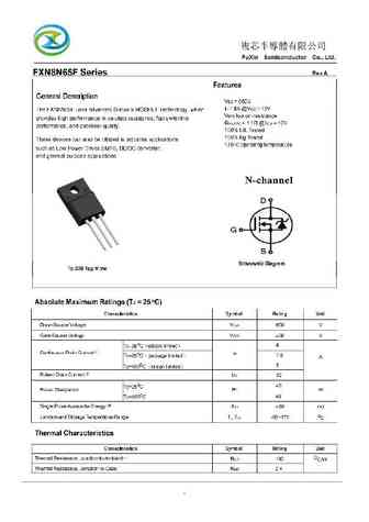
fxn8n65f.pdf
1 FuXin Semiconductor Co., Ltd. Electrical Characteristics (TJ =25oC) Characteristics Symbol Test Condition Min Typ Max Unit Static Characteristics Drain-Source Breakdown Voltage BVDSS ID = 250 A, VGS = 0V 650 - - V Gate Threshold Voltage VGS(th) 2.0 3.0 4.0 VDS = VGS, ID = 250 A Drain Cut-Off Current IDSS VDS = 650V, VGS = 0V - - 1 A Ga... See More ⇒
h8n65p h8n65f.pdf
8N65 Series N-Channel MOSFET 7.5A, 650V, N H FQP8N65C H8N65P P TO-220AB HAOHAI 50Pcs 1000Pcs 5000Pcs 8N65 FQPF8N65C H8N65F F TO-220FP 8N65 Series Pin Assignment Features ID=7.5A Originative New Design ... See More ⇒
aok18n65.pdf
isc N-Channel MOSFET Transistor AOK18N65 FEATURES Drain Current I = 18A@ T =25 D C Drain Source Voltage- V =650V(Min) DSS Static Drain-Source On-Resistance R =0.39 (Max) DS(on) 100% avalanche tested Minimum Lot-to-Lot variations for robust device performance and reliable operation DESCRIPTION Designed for use in switch mode power supplies and general purpos... See More ⇒
aotf18n65.pdf
isc N-Channel MOSFET Transistor AOTF18N65 FEATURES Drain Current I = 18A@ T =25 D C Drain Source Voltage- V =650V(Min) DSS Static Drain-Source On-Resistance R =0.39 (Max) DS(on) 100% avalanche tested Minimum Lot-to-Lot variations for robust device performance and reliable operation DESCRIPTION Designed for use in switch mode power supplies and general purpo... See More ⇒
stp8n65m5.pdf
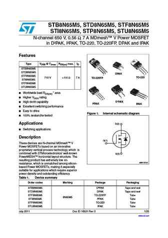
INCHANGE Semiconductor Isc N-Channel MOSFET Transistor STP8N65M5 FEATURES Higher V rating DSS Excellent switching performance Easy to drive 100% avalanche tested Minimum Lot-to-Lot variations for robust device performance and reliable operation APPLICATIONS Switching applications ABSOLUTE MAXIMUM RATINGS(T =25 ) a SYMBOL PARAMETER VALUE UNIT V Drain-Source Vol... See More ⇒
stf18n65m5.pdf
INCHANGE Semiconductor Isc N-Channel MOSFET Transistor STF18N65M5 FEATURES Higher V rating DSS Excellent switching performance 100% avalanche tested Minimum Lot-to-Lot variations for robust device performance and reliable operation APPLICATIONS Switching applications ABSOLUTE MAXIMUM RATINGS(T =25 ) a SYMBOL PARAMETER VALUE UNIT V Drain-Source Voltage 650 V DSS ... See More ⇒
aot8n65.pdf
isc N-Channel MOSFET Transistor AOT8N65 FEATURES Drain Current I = 8A@ T =25 D C Drain Source Voltage- V = 650V(Min) DSS Static Drain-Source On-Resistance R = 1.15 (Max) DS(on) 100% avalanche tested Minimum Lot-to-Lot variations for robust device performance and reliable operation DESCRIPTION Designed for use in switch mode power supplies and general purpos... See More ⇒
std18n65m5.pdf
INCHANGE Semiconductor Isc N-Channel MOSFET Transistor STD18N65M5 FEATURES Higher V rating DSS Excellent switching performance 100% avalanche tested Minimum Lot-to-Lot variations for robust device performance and reliable operation APPLICATIONS Switching applications ABSOLUTE MAXIMUM RATINGS(T =25 ) a SYMBOL PARAMETER VALUE UNIT V Drain-Source Voltage 650 V DSS ... See More ⇒
stf8n65m5.pdf
INCHANGE Semiconductor Isc N-Channel MOSFET Transistor STF8N65M5 FEATURES Excellent switching performance Easy to drive 100% avalanche tested Minimum Lot-to-Lot variations for robust device performance and reliable operation APPLICATIONS Switching applications ABSOLUTE MAXIMUM RATINGS(T =25 ) a SYMBOL PARAMETER VALUE UNIT V Drain-Source Voltage 650 V DSS V Gate-... See More ⇒
aotf8n65.pdf
isc N-Channel MOSFET Transistor AOTF8N65 FEATURES Drain Current I = 8A@ T =25 D C Drain Source Voltage- V = 650V(Min) DSS Static Drain-Source On-Resistance R = 1.15 (Max) DS(on) 100% avalanche tested Minimum Lot-to-Lot variations for robust device performance and reliable operation DESCRIPTION Designed for use in switch mode power supplies and general purpo... See More ⇒
dmg8n65sct.pdf
isc N-Channel MOSFET Transistor DMG8N65SCT FEATURES Drain Current I = 8.0A@ T =25 D C Drain Source Voltage- V = 650V(Min) DSS Static Drain-Source On-Resistance R = 1.3 (Max) DS(on) 100% avalanche tested Minimum Lot-to-Lot variations for robust device performance and reliable operation DESCRIPTION Designed for use in switch mode power supplies and general pu... See More ⇒
Detailed specifications: 10N70 , 12N70 , 15N70 , 6N65Z , 7N65A , 7N65 , 7N65Z , 7N65K , 4N60 , 9N65 , 10N65 , 10N65Z , 10N65K , 15N65 , 18N65 , 20N65 , 22N65 .
Keywords - 8N65 MOSFET specs
8N65 cross reference
8N65 equivalent finder
8N65 pdf lookup
8N65 substitution
8N65 replacement
Step-by-step guide to finding a MOSFET replacement. Cross-reference parts and ensure compatibility for your repair or project.
🌐 : EN ES РУ
LIST
Last Update
MOSFET: AON5802 | AOSS62934 | AOSN21319C | AONS66966 | AONR62992 | AON7400B | AON6578 | AO3480C | AO3400C | HAF1008S
Popular searches
2n2222a datasheet | bd136 | tl431 datasheet | 2sd526 | 2n4403 transistor equivalent | 2sc1318 | 2n3055 transistor equivalent | 2sc1740
