2N40 Specs and Replacement
Type Designator: 2N40
Type of Transistor: MOSFET
Type of Control Channel: N-Channel
Absolute Maximum Ratings
Pd ⓘ - Maximum Power Dissipation: 25 W
|Vds|ⓘ - Maximum Drain-Source Voltage: 400 V
|Vgs|ⓘ - Maximum Gate-Source Voltage: 30 V
|Id| ⓘ - Maximum Drain Current: 2 A
Tj ⓘ - Maximum Junction Temperature: 150 °C
Electrical Characteristics
tr ⓘ - Rise Time: 25 nS
Cossⓘ - Output Capacitance: 44 pF
RDSonⓘ - Maximum Drain-Source On-State Resistance: 3 Ohm
Package: TO-220
2N40 substitution
- MOSFET ⓘ Cross-Reference Search
2N40 datasheet
2n40.pdf
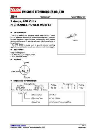
UNISONIC TECHNOLOGIES CO., LTD 2N40 Preliminary Power MOSFET 2 Amps, 400 Volts N-CHANNEL POWER MOSFET DESCRIPTION The UTC 2N40 is an N-channel mode power MOSFET using UTC s advanced technology to provide customers with a minimum on-state resistance, stable off state characteristics and superior switching performance. It also can withstand high energy pulse in the avalanc... See More ⇒
hgth12n40c1d hgth12n40e1d hgth12n50c1d hgth12n50e1d.pdf
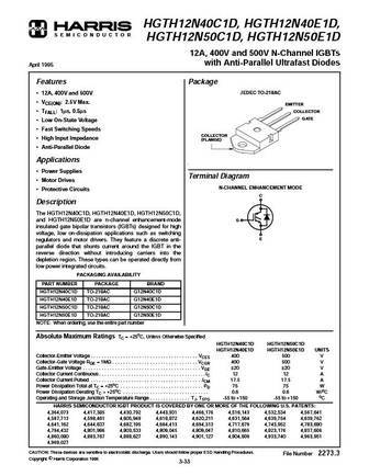
HGTH12N40C1D, HGTH12N40E1D, S E M I C O N D U C T O R HGTH12N50C1D, HGTH12N50E1D 12A, 400V and 500V N-Channel IGBTs with Anti-Parallel Ultrafast Diodes April 1995 Features Package JEDEC TO-218AC 12A, 400V and 500V VCE(ON) 2.5V Max. EMITTER TFALL 1 s, 0.5 s COLLECTOR GATE Low On-State Voltage Fast Switching Speeds COLLECTOR High Input Impedance (FLANG... See More ⇒
hgth12n40c1 hgth12n40e1 hgth12n50c1 hgth12n50e1 hgtm12n40c1 hgtm12n40e1 hgtm12n50c1 hgtm12n50e1 hgtp10n40c1 hgtp10n40e1 hgtp10n50c1 hgtp10n50e1.pdf
... See More ⇒
hgth12n40c1 hgth12n40e1 hgth12n50c1 hgth12n50e1 hgtp10n40c1 hgtp10n40e1 hgtp10n50c1 hgtp10n50e1.pdf
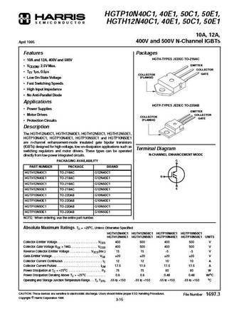
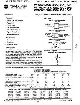
HGTP10N40C1, 40E1, 50C1, 50E1, S E M I C O N D U C T O R HGTH12N40C1, 40E1, 50C1, 50E1 10A, 12A, 400V and 500V N-Channel IGBTs April 1995 Features Packages HGTH-TYPES JEDEC TO-218AC 10A and 12A, 400V and 500V EMITTER VCE(ON) 2.5V Max. COLLECTOR TFI 1 s, 0.5 s GATE COLLECTOR (FLANGE) Low On-State Voltage Fast Switching Speeds High Input Impedance ... See More ⇒
mtp2n40erev0bx.pdf
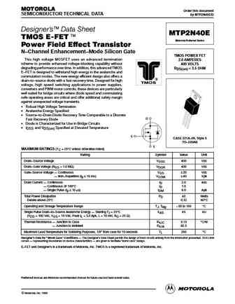
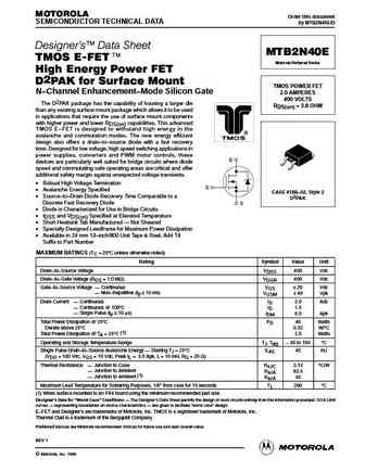
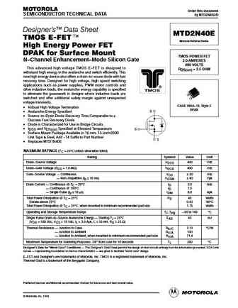
MOTOROLA Order this document SEMICONDUCTOR TECHNICAL DATA by MTP2N40E/D Designer's Data Sheet MTP2N40E TMOS E-FET. Motorola Preferred Device Power Field Effect Transistor N Channel Enhancement Mode Silicon Gate TMOS POWER FET This high voltage MOSFET uses an advanced termination 2.0 AMPERES scheme to provide enhanced voltage blocking capability without 400 VOLTS degra... See More ⇒
mtd2n40erev0x.pdf

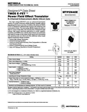
MOTOROLA Order this document SEMICONDUCTOR TECHNICAL DATA by MTD2N40E/D Designer's Data Sheet MTD2N40E TMOS E-FET. Motorola Preferred Device High Energy Power FET DPAK for Surface Mount TMOS POWER FET N Channel Enhancement Mode Silicon Gate 2.0 AMPERES 400 VOLTS This advanced high voltage TMOS E FET is designed to RDS(on) = 3.5 OHM withstand high energy in the avalanc... See More ⇒
mtb2n40e.pdf
MOTOROLA Order this document SEMICONDUCTOR TECHNICAL DATA by MTB2N40E/D Designer's Data Sheet MTB2N40E TMOS E-FET. Motorola Preferred Device High Energy Power FET D2PAK for Surface Mount TMOS POWER FET N Channel Enhancement Mode Silicon Gate 2.0 AMPERES 400 VOLTS The D2PAK package has the capability of housing a larger die RDS(on) = 3.8 OHM than any existing surface mou... See More ⇒
mtp2n40e.pdf
MOTOROLA Order this document SEMICONDUCTOR TECHNICAL DATA by MTP2N40E/D Designer's Data Sheet MTP2N40E TMOS E-FET. Motorola Preferred Device Power Field Effect Transistor N Channel Enhancement Mode Silicon Gate TMOS POWER FET This high voltage MOSFET uses an advanced termination 2.0 AMPERES scheme to provide enhanced voltage blocking capability without 400 VOLTS degra... See More ⇒
mtd2n40e.pdf
MOTOROLA Order this document SEMICONDUCTOR TECHNICAL DATA by MTD2N40E/D Designer's Data Sheet MTD2N40E TMOS E-FET. Motorola Preferred Device High Energy Power FET DPAK for Surface Mount TMOS POWER FET N Channel Enhancement Mode Silicon Gate 2.0 AMPERES 400 VOLTS This advanced high voltage TMOS E FET is designed to RDS(on) = 3.5 OHM withstand high energy in the avalanc... See More ⇒
php2n40 1.pdf
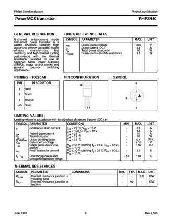
Philips Semiconductors Product specification PowerMOS transistor PHP2N40 GENERAL DESCRIPTION QUICK REFERENCE DATA N-channel enhancement mode SYMBOL PARAMETER MAX. UNIT field-effect power transistor in a plastic envelope featuring high VDS Drain-source voltage 400 V avalanche energy capability, stable ID Drain current (DC) 2.5 A off-state characteristics, fast Ptot Total power dissipati... See More ⇒
php2n40e 1.pdf
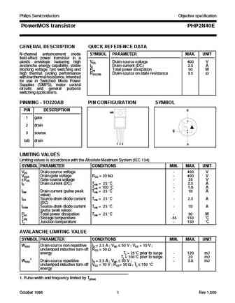
Philips Semiconductors Objective specification PowerMOS transistor PHP2N40E GENERAL DESCRIPTION QUICK REFERENCE DATA N-channel enhancement mode SYMBOL PARAMETER MAX. UNIT field-effect power transistor in a plastic envelope featuring high VDS Drain-source voltage 400 V avalanche energy capability, stable ID Drain current (DC) 2.5 A blocking voltage, fast switching and Ptot Total power d... See More ⇒
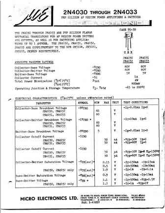
2n4031 2n4033.pdf
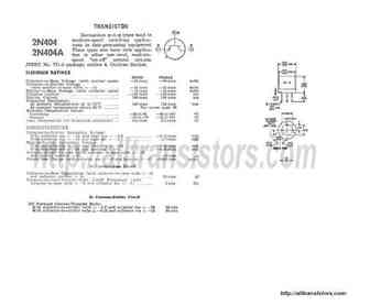
DISCRETE SEMICONDUCTORS DATA SHEET book, halfpage M3D111 2N4031; 2N4033 PNP medium power transistors 1997 May 22 Product specification Supersedes data of September 1994 File under Discrete Semiconductors, SC04 Philips Semiconductors Product specification PNP medium power transistors 2N4031; 2N4033 FEATURES PINNING High current (max. 1 A) PIN DESCRIPTION Low voltage (max.... See More ⇒
2n4036.pdf
DISCRETE SEMICONDUCTORS DATA SHEET book, halfpage M3D111 2N4036 PNP switching transistor 1997 Jun 19 Product specification Supersedes data of September 1994 File under Discrete Semiconductors, SC04 Philips Semiconductors Product specification PNP switching transistor 2N4036 FEATURES PINNING High current (max. 1 A) PIN DESCRIPTION Low voltage (max. 65 V). 1 emitter 2 ba... See More ⇒
phx2n40e 1.pdf
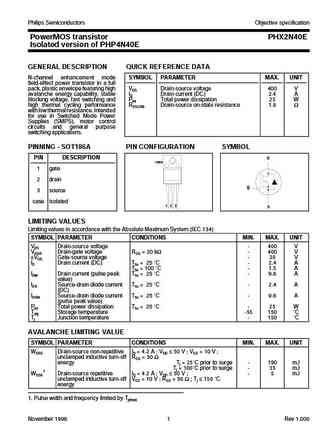
Philips Semiconductors Objective specification PowerMOS transistor PHX2N40E Isolated version of PHP4N40E GENERAL DESCRIPTION QUICK REFERENCE DATA N-channel enhancement mode SYMBOL PARAMETER MAX. UNIT field-effect power transistor in a full pack, plastic envelope featuring high VDS Drain-source voltage 400 V avalanche energy capability, stable ID Drain current (DC) 2.4 A blocking volt... See More ⇒
2n4033.pdf
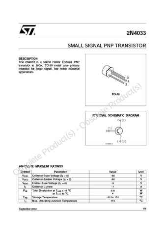
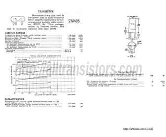
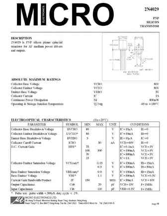
2N4033 SMALL SIGNAL PNP TRANSISTOR DESCRIPTION The 2N4033 is a silicon Planar Epitaxial PNP transistor in Jedec TO-39 metal case primary intended for large signal, low noise industrial applications. TO-39 INTERNAL SCHEMATIC DIAGRAM ABSOLUTE MAXIMUM RATINGS Symbol Parameter Value Unit VCBO Collector-Base Voltage (IE = 0) -80 V VCEO Collector-Emitter Voltage (IB = 0) -80 V V Emi... See More ⇒
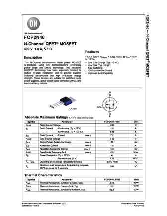
fqp2n40.pdf
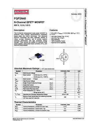
October 2013 FQP2N40 N-Channel QFET MOSFET 400 V, 1.8 A, 5.8 Description Features This N-Channel enhancement mode power MOSFET is 1.8 A, 400 V, RDS(on) = 5.8 (Max.) @ VGS = 10 V, ID = 0.9 A produced using Fairchild Semiconductor s proprietary planar stripe and DMOS technology. This advanced Low Gate Charge (Typ. 4.0 nC) MOSFET technology has been especially ta... See More ⇒
fqpf2n40.pdf
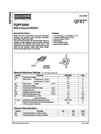
April 2000 TM QFET QFET QFET QFET 400V N-ChanneI MOSFET GeneraI Description Features These N-Channel enhancement mode power field effect 1.1A, 400V, RDS(on) = 5.8 @VGS = 10 V transistors are produced using Fairchild s proprietary, Low gate charge ( typical 4.0 nC) planar stripe, DMOS technology. Low Crss ( typical 3.0 pF) This advanced technology has bee... See More ⇒
fqd2n40tf fqd2n40tm.pdf
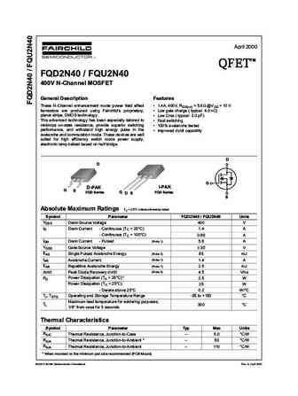
April 2000 TM QFET QFET QFET QFET FQD2N40 / FQU2N40 400V N-ChanneI MOSFET GeneraI Description Features These N-Channel enhancement mode power field effect 1.4A, 400V, RDS(on) = 5.8 @VGS = 10 V transistors are produced using Fairchild s proprietary, Low gate charge ( typical 4.0 nC) planar stripe, DMOS technology. Low Crss ( typical 3.0 pF) This advanced technolog... See More ⇒
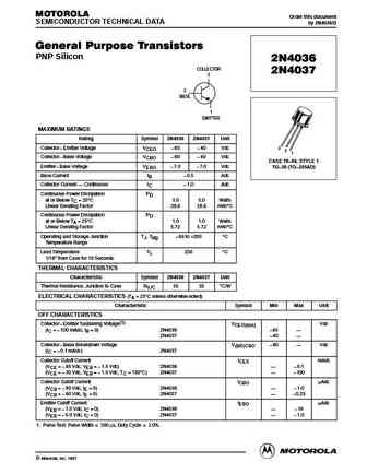
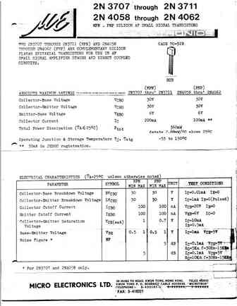
2n4036 2n4037.pdf
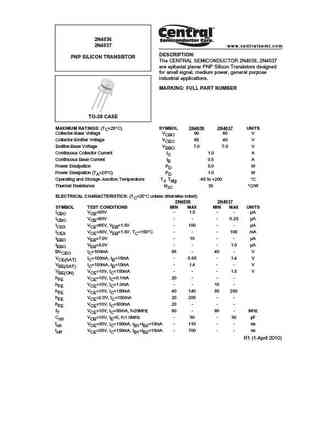
2N4036 2N4037 www.centralsemi.com DESCRIPTION PNP SILICON TRANSISTOR The CENTRAL SEMICONDUCTOR 2N4036, 2N4037 are epitaxial planar PNP Silicon Transistors designed for small signal, medium power, general purpose industrial applications. MARKING FULL PART NUMBER TO-39 CASE MAXIMUM RATINGS (TC=25 C) SYMBOL 2N4036 2N4037 UNITS Collector-Base Voltage VCBO 90 60 V Collector-Emitt... See More ⇒
ndd02n40 ndt02n40.pdf
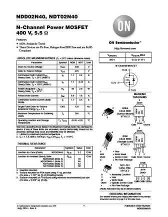
NDD02N40, NDT02N40 N-Channel Power MOSFET 400 V, 5.5 W Features 100% Avalanche Tested These Devices are Pb-Free, Halogen Free/BFR Free and are RoHS http //onsemi.com Compliant V(BR)DSS RDS(ON) MAX ABSOLUTE MAXIMUM RATINGS (TJ = 25 C unless otherwise noted) 400 V 5.5 W @ 10 V Parameter Symbol NDD NDT Unit N-Channel MOSFET Drain-to-Source Voltage VDSS 400 V D (2) Gate-to-S... See More ⇒
fqp2n40.pdf
FQP2N40 N-Channel QFET MOSFET 400 V, 1.8 A, 5.8 Features 1.8 A, 400 V, RDS(on) = 5.8 (Max.) @ VGS = 10 V, Description ID = 0.9 A This N-Channel enhancement mode power MOSFET Low Gate Charge (Typ. 4.0 nC) is produced using ON Semiconductor s proprietary Low Crss (Typ. 3.0 pF) planar stripe and DMOS technology. This advanced Fast Switching MOSFET technolog... See More ⇒
12n40.pdf
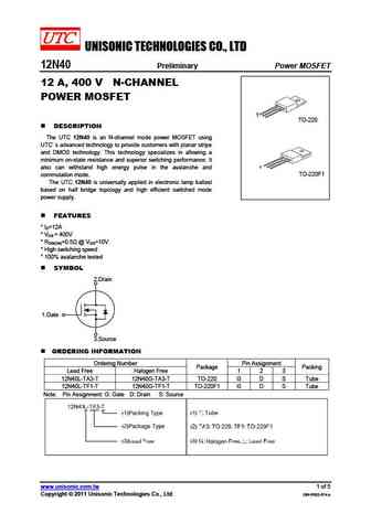
UNISONIC TECHNOLOGIES CO., LTD 12N40 Preliminary Power MOSFET 12 A, 400 V N-CHANNEL POWER MOSFET 1 TO-220 DESCRIPTION The UTC 12N40 is an N-channel mode power MOSFET using UTC s advanced technology to provide customers with planar stripe and DMOS technology. This technology specializes in allowing a minimum on-state resistance and superior switching performance. It 1 als... See More ⇒
2n4000.pdf
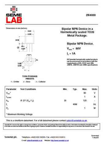
2N4000 Dimensions in mm (inches). Bipolar NPN Device in a 8.51 (0.34) 9.40 (0.37) Hermetically sealed TO39 7.75 (0.305) 8.51 (0.335) Metal Package. 6.10 (0.240) 6.60 (0.260) Bipolar NPN Device. 0.89 max. (0.035) 12.70 (0.500) min. 0.41 (0.016) 0.53 (0.021) VCEO = 80V dia. IC = 1A 5.08 (0.200) typ. 2.54 All Semelab hermetically sealed products 2 (0.100) 1 3 ... See More ⇒
2n4028.pdf
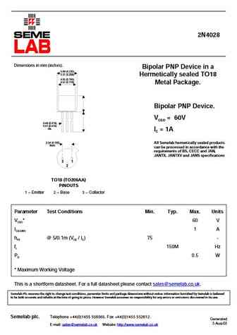
2N4028 Dimensions in mm (inches). Bipolar PNP Device in a 5.84 (0.230) 5.31 (0.209) Hermetically sealed TO18 4.95 (0.195) 4.52 (0.178) Metal Package. Bipolar PNP Device. VCEO = 60V 0.48 (0.019) 0.41 (0.016) dia. IC = 1A 2.54 (0.100) All Semelab hermetically sealed products Nom. can be processed in accordance with the requirements of BS, CECC and JAN, JANTX, JANTX... See More ⇒
2n4001.pdf

2N4001 Dimensions in mm (inches). Bipolar NPN Device in a 8.51 (0.34) 9.40 (0.37) Hermetically sealed TO39 7.75 (0.305) 8.51 (0.335) Metal Package. 6.10 (0.240) 6.60 (0.260) Bipolar NPN Device. 0.89 max. (0.035) 12.70 (0.500) min. 0.41 (0.016) 0.53 (0.021) VCEO = 100V dia. IC = 1A 5.08 (0.200) typ. 2.54 All Semelab hermetically sealed products 2 (0.100) 1 3... See More ⇒
2n4027.pdf

2N4027 Dimensions in mm (inches). Bipolar PNP Device in a 5.84 (0.230) 5.31 (0.209) Hermetically sealed TO18 4.95 (0.195) 4.52 (0.178) Metal Package. Bipolar PNP Device. VCEO = 80V 0.48 (0.019) 0.41 (0.016) dia. IC = 1A 2.54 (0.100) All Semelab hermetically sealed products Nom. can be processed in accordance with the requirements of BS, CECC and JAN, JANTX, JANTX... See More ⇒
2n4030 1 2 3.pdf
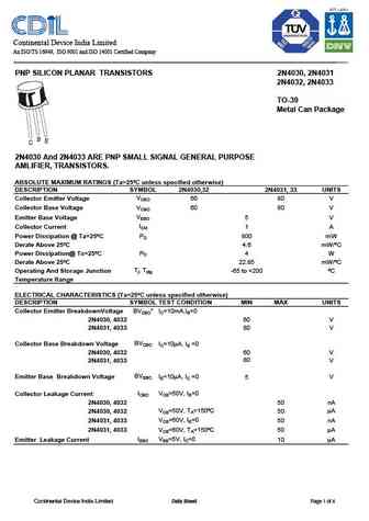
Continental Device India Limited An ISO/TS 16949, ISO 9001 and ISO 14001 Certified Company PNP SILICON PLANAR TRANSISTORS 2N4030, 2N4031 2N4032, 2N4033 TO-39 Metal Can Package 2N4030 And 2N4033 ARE PNP SMALL SIGNAL GENERAL PURPOSE AMLIFIER, TRANSISTORS. ABSOLUTE MAXIMUM RATINGS (Ta=25 C unless specified otherwise) DESCRIPTION SYMBOL 2N4030,32 2N4031, 33 UNITS VCEO Collector Emitter... See More ⇒
2n4037.pdf
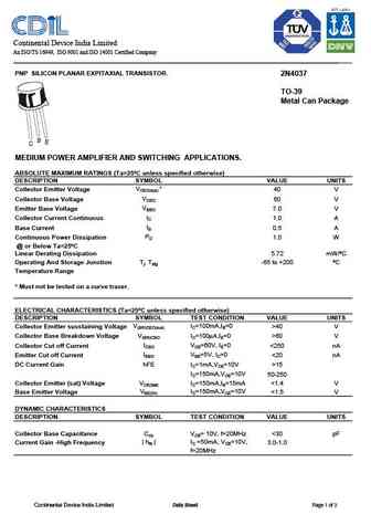
Continental Device India Limited An ISO/TS 16949, ISO 9001 and ISO 14001 Certified Company PNP SILICON PLANAR EXPITAXIAL TRANSISTOR. 2N4037 TO-39 Metal Can Package MEDIUM POWER AMPLIFIER AND SWITCHING APPLICATIONS. ABSOLUTE MAXIMUM RATINGS (Ta=25 C unless specified otherwise) DESCRIPTION SYMBOL VALUE UNITS VCEO(sus) * Collector Emitter Voltage 40 V VCBO Collector Base Voltage 60 V ... See More ⇒
2n4036.pdf
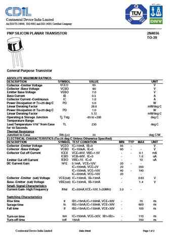
Continental Device India Limited An ISO/TS 16949, ISO 9001 and ISO 14001 Certified Company PNP SILICON PLANAR TRANSISTOR 2N4036 TO-39 General Purpose Transistor ABSOLUTE MAXIMUM RATINGS DESCRIPTION SYMBOL VALUE UNIT Collector -Emitter Voltage VCEO 65 V Collector -Base Voltage VCBO 90 V Emitter Base Voltage VEBO 7.0 V Base Current IB 0.5 A Collector Current -Continuous IC 1.0 A Powe... See More ⇒
kmb012n40da.pdf
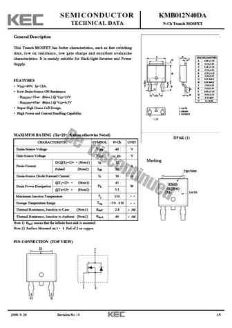
SEMICONDUCTOR KMB012N40DA TECHNICAL DATA N-Ch Trench MOSFET General Description This Trench MOSFET has better characteristics, such as fast switching time, low on resistance, low gate charge and excellent avalanche A K DIM MILLIMETERS characteristics. It is mainly suitable for Back-light Inverter and Power L C D _ A 6.60 + 0.20 _ B 6.10 + 0.20 Supply. _ C 5.34 + 0.30 _ D 0.70 +... See More ⇒
mx2n4091 mx2n4092 mx2n4093.pdf
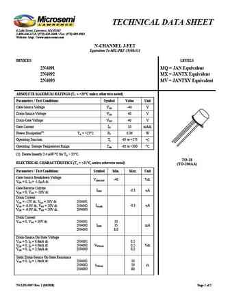
TECHNICAL DATA SHEET 6 Lake Street, Lawrence, MA 01841 1-800-446-1158 / (978) 620-2600 / Fax (978) 689-0803 Website http //www.microsemi.com N-CHANNEL J-FET Equivalent To MIL-PRF-19500/431 DEVICES LEVELS 2N4091 MQ = JAN Equivalent 2N4092 MX = JANTX Equivalent 2N4093 MV = JANTXV Equivalent ABSOLUTE MAXIMUM RATINGS (TC = +25 C unless otherwise noted) Parameters / Test C... See More ⇒
2n4033ub.pdf
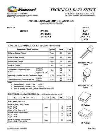
TECHNICAL DATA SHEET 6 Lake Street, Lawrence, MA 01841 Gort Road Business Park, Ennis, Co. Clare, Ireland. 1-800-446-1158 / (978) 620-2600 / Fax (978) 689-0803 Tel +353 (0) 65 6840044 Fax +353 (0) 65 6822298 Website http //www.microsemi.com PNP SILICON SWITCHING TRANSISTOR Qualified per MIL-PRF-19500/512 DEVICES LEVELS 2N4029 2N4033 JAN 2N4033UA JANTX 2N4033UB JANTXV JANS ... See More ⇒
2n4091 2n4092 2n4093.pdf
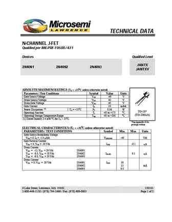
TECHNICAL DATA N-CHANNEL J-FET Qualified per MIL-PRF-19500/431 Devices Qualified Level JANTX 2N4091 2N4092 2N4093 JANTXV ABSOLUTE MAXIMUM RATINGS (T = +250C unless otherwise noted) A Parameters / Test Conditions Symbol Value Units Gate-Source Voltage V -40 V GS Drain-Source Voltage V 40 V DS Drain-Gate Voltage VDG 40 V Gate Current I 10 mAdc G (1) Power Dissipa... See More ⇒
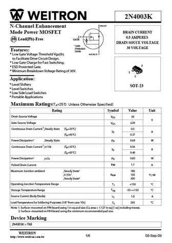
2n4003k.pdf
2N4003K 3 DRAIN N-Channel Enhancement DRAIN CURRENT Mode Power MOSFET 1 0.5 AMPERES GATE P b Lead(Pb)-Free * DRAIN SOUCE VOLTAGE * Gate 30 VOLTAGE Pretection Features Diode SOURCE 2 * Low Gate Voltage Threshold Vgs(th) to Facilitate Drive Circuit Design. * Low Gate Charge for Fast Switching. 3 * ESD Protected Gate. * Minimum Breakdown Voltage Rating of 30V. 1 2 ... See More ⇒
2n4003nlt1.pdf
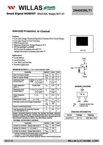
FM120-M WILLAS THRU 2N4003NLT1 Small Signal MOSFET 30V,0.56A, Single, SOT-23 FM1200-M 1.0A SURFACE MOUNT SCHOTTKY BARRIER RECTIFIERS -20V- 200V SOD-123 PACKAGE Pb Free Product Package outline Features Batch process design, excellent power dissipation offers better reverse leakage current and thermal resistance. SOD-123H Low profile surface mounted application in ord... See More ⇒
aot12n40.pdf
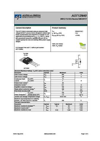
AOT12N40 400V,11A N-Channel MOSFET General Description Product Summary VDS 500V@150 The AOT12N40 is fabricated using an advanced high voltage MOSFET process that is designed to deliver high ID (at VGS=10V) 11A levels of performance and robustness in popular AC-DC RDS(ON) (at VGS=10V) ... See More ⇒
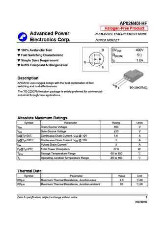
ap02n40h.pdf
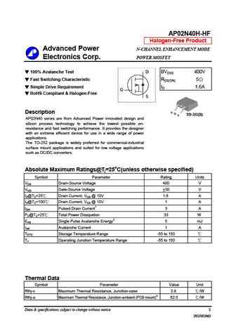
AP02N40H-HF Halogen-Free Product Advanced Power N-CHANNEL ENHANCEMENT MODE Electronics Corp. POWER MOSFET 100% Avalanche Test D BVDSS 400V Fast Switching Characteristic RDS(ON) 5 Simple Drive Requirement ID 1.6A G RoHS Compliant & Halogen-Free S G Description D TO-252(H) S AP02N40 series are from Advanced Power innovated design and silicon process technology to... See More ⇒
ap02n40h-hf ap02n40j-hf.pdf
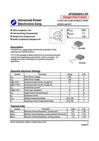
AP02N40H/J-HF Halogen-Free Product Advanced Power N-CHANNEL ENHANCEMENT MODE Electronics Corp. POWER MOSFET 100% Avalanche Test D BVDSS 400V Fast Switching Characteristic RDS(ON) 5 Simple Drive Requirement ID 1.6A G RoHS Compliant & Halogen-Free S G Description D TO-252(H) S AP02N40 uses rugged design with the best combination of fast switching and cost-effecti... See More ⇒
ap02n40p.pdf
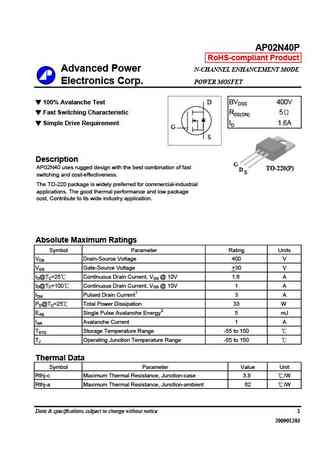
AP02N40P RoHS-compliant Product Advanced Power N-CHANNEL ENHANCEMENT MODE Electronics Corp. POWER MOSFET 100% Avalanche Test D BVDSS 400V Fast Switching Characteristic RDS(ON) 5 Simple Drive Requirement ID 1.6A G S Description G AP02N40 uses rugged design with the best combination of fast TO-220(P) D S switching and cost-effectiveness. The TO-220 package is widely ... See More ⇒
ap02n40k-hf.pdf
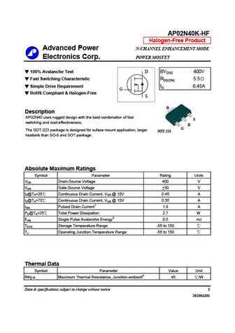
AP02N40K-HF Halogen-Free Product Advanced Power N-CHANNEL ENHANCEMENT MODE Electronics Corp. POWER MOSFET 100% Avalanche Test D BVDSS 400V Fast Switching Characteristic RDS(ON) 5.5 Simple Drive Requirement ID 0.45A G RoHS Compliant & Halogen-Free S D Description AP02N40 uses rugged design with the best combination of fast S switching and cost-effectiveness. D G... See More ⇒
ap02n40i-hf.pdf
AP02N40I-HF Halogen-Free Product Advanced Power N-CHANNEL ENHANCEMENT MODE Electronics Corp. POWER MOSFET 100% Avalanche Test D BVDSS 400V Fast Switching Characteristic RDS(ON) 5 Simple Drive Requirement ID 1.6A G RoHS Compliant & Halogen-Free S Description AP02N40 uses rugged design with the best combination of fast G switching and cost-effectiveness. D TO-220CF... See More ⇒
msf2n40.pdf
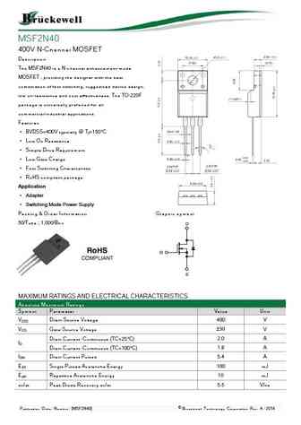
MSF2N40 400V N-Channel MOSFET Description The MSF2N40 is a N-channel enhancement-mode MOSFET , providing the designer with the best combination of fast switching, ruggedized device design, low on-resistance and cost effectiveness. The TO-220F package is universally preferred for all commercial-industrial applications Features BVDSS=400V typically @ Tj=150 C Low On... See More ⇒
2n4006 2n4007 2n4008 2n4009 2n4010 2n4011.pdf
www.DataSheet.co.kr Datasheet pdf - http //www.DataSheet4U.net/ ... See More ⇒
swsi2n40dc swd2n40dc.pdf
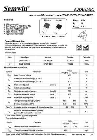
SW2N40DC N-channel Enhanced mode TO-251S/TO-252 MOSFET Features TO-251S BVDSS 400V TO-252 ID 2A High ruggedness Low RDS(ON) (Typ 2.8 )@VGS=10V RDS(ON) 2.8 Low Gate Charge (Typ 6.8nC) Improved dv/dt Capability 2 1 100% Avalanche Tested 1 2 2 3 Application DC-DC,LED 3 1 1. Gate 2. Drain 3. Source 3 General Description ... See More ⇒
swc2n40d swsa2n40d.pdf
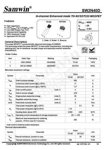
SW2N40D N-channel Enhanced mode TO-92/SOT223 MOSFET Features SOT223 TO-92 BVDSS 400V ID 2A High ruggedness Low RDS(ON) (Typ 2.8 )@VGS=10V RDS(ON) 2.8 Low Gate Charge (Typ 7nC) Improved dv/dt Capability 2 100% Avalanche Tested 1 1 2 2 Application DC-DC,LED 3 3 1 1. Gate 2. Drain 3. Source General Description 3 T... See More ⇒
tmt2n40g.pdf
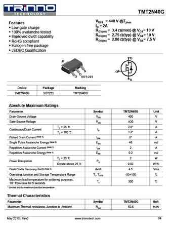
TMT2N40G VDSS = 440 V @Tjmax Features ID = 2A Low gate charge RDS(on) = 3.4 W(max) @ VGS= 10 V 100% avalanche tested RDS(on) = 2.75 W(typ) @ VGS= 10 V Improved dv/dt capability RDS(on) = 2.80 W(typ) @ VGS= 7.5 V RoHS compliant Halogen free package JEDEC Qualification D D S G D G S Device Package Marking TMT2N40G SOT223 TMT2N40G Absolute Maximum Ra... See More ⇒
tmd2n40 tmu2n40.pdf
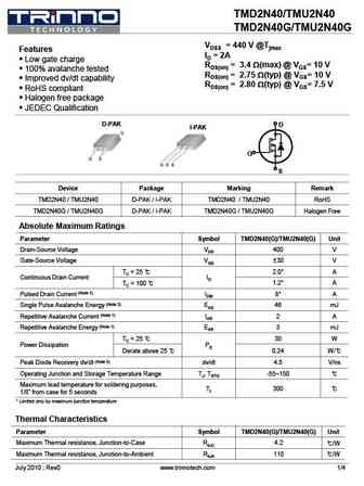
TMD2N40/TMU2N40 TMD2N40G/TMU2N40G VDSS = 440 V @Tjmax Features ID = 2A Low gate charge RDS(on) = 3.4 W(max) @ VGS= 10 V 100% avalanche tested RDS(on) = 2.75 W(typ) @ VGS= 10 V Improved dv/dt capability RDS(on) = 2.80 W(typ) @ VGS= 7.5 V RoHS compliant Halogen free package JEDEC Qualification D-PAK D I-PAK G S Device Package Marking Remark TMD2N40 / ... See More ⇒
2n3906 2n3973 2n3974 2n3975 2n3976 2n4058 2n4059 2n4060 2n4061 2n4062 2n4123 2n4124 2n4125 2n4126 2n4256 2n4264.pdf
... See More ⇒
2n4070.pdf
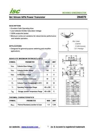
isc Silicon NPN Power Transistor 2N4070 DESCRIPTION Excellent Safe Operating Area Low Collector-Emitter Saturation Voltage 100% avalanche tested Minimum Lot-to-Lot variations for robust device performance and reliable operation. APPLICATIONS Designed for general-purpose switching and amplifier applications ABSOLUTE MAXIMUM RATINGS(T =25 ) a SYMBOL PARAMETER VALUE UNIT V... See More ⇒
aot12n40.pdf
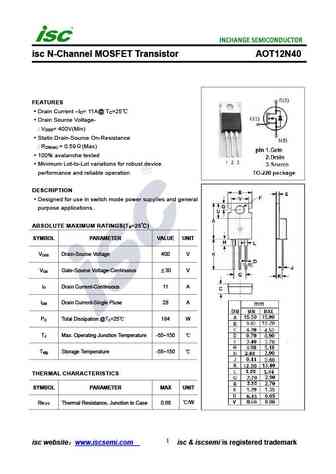
isc N-Channel MOSFET Transistor AOT12N40 FEATURES Drain Current I = 11A@ T =25 D C Drain Source Voltage- V = 400V(Min) DSS Static Drain-Source On-Resistance R = 0.59 (Max) DS(on) 100% avalanche tested Minimum Lot-to-Lot variations for robust device performance and reliable operation DESCRIPTION Designed for use in switch mode power supplies and general purp... See More ⇒
ap12n40f ap12n40p.pdf
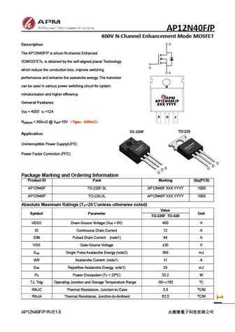
AP12N40FIP 400V N-Channel Enhancement Mode MOSFET Description The AP12N40F/P is silicon N-channel Enhanced VDMOSFETs, is obtained by the self-aligned planar Technology which reduce the conduction loss, improve switching performance and enhance the avalanche energy. The transistor can be used in various power switching circuit for system miniaturization and higher efficiency. ... See More ⇒
Detailed specifications: 3N50Z , 4N50 , 5N50 , 5N50K , 6N50 , 7N50 , 8N50 , 1N40 , 12N60 , 3N40 , 4N40 , 5N40 , 6N40 , 7N40 , 8N40 , 9N40 , 10N40 .
Keywords - 2N40 MOSFET specs
2N40 cross reference
2N40 equivalent finder
2N40 pdf lookup
2N40 substitution
2N40 replacement
Need a MOSFET replacement? Our guide shows you how to find a perfect substitute by comparing key parameters and specs
🌐 : EN ES РУ

LIST
Last Update
MOSFET: HAF1008S | HAF1008L | EMZB08P03H | CS30N20FA9R | AOT66613L | AOSP21313C | AOSP21311C | AOB66918L | AO3415C | AOTF20N40L
Popular searches
2sb817 | mn2488 datasheet | c2026 transistor | 2n3903 transistor | 2n4360 | 2n2613 | c2166 transistor | 2sd330