50N06 Datasheet. Specs and Replacement
The 50N06 is an N-channel MOSFET designed for high-speed switching and low on-resistance applications. It features a maximum drain current of 50A and a drain-source voltage of 60V, making it suitable for power management, motor control, DC-DC converters. With a low gate threshold voltage and efficient thermal performance, the 50N06 provides reliable operation in demanding electronic circuits.
Type Designator: 50N06 📄📄
Type of Transistor: MOSFET
Type of Control Channel: N-Channel
Absolute Maximum Ratings
Pd ⓘ - Maximum Power Dissipation: 120 W
|Vds|ⓘ - Maximum Drain-Source Voltage: 60 V
|Vgs|ⓘ - Maximum Gate-Source Voltage: 20 V
|Id| ⓘ - Maximum Drain Current: 50 A
Tj ⓘ - Maximum Junction Temperature: 150 °C
Electrical Characteristics
tr ⓘ - Rise Time: 100 nS
Cossⓘ - Output Capacitance: 430 pF
RDSonⓘ - Maximum Drain-Source On-State Resistance: 0.018 Ohm
📄📄 Copy
50N06 substitution
- MOSFET ⓘ Cross-Reference Search
50N06 datasheet
50n06.pdf
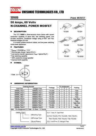
UNISONIC TECHNOLOGIES CO., LTD 50N06 Power MOSFET 50 Amps, 60 Volts N-CHANNEL POWER MOSFET 1 1 DESCRIPTION TO-263 TO-251 The UTC 50N06 is three-terminal silicon device with current conduction capability of about 50A, fast switching speed. Low on-state resistance, breakdown voltage rating of 60V, and max threshold voltages of 4 volt. 1 1 It is mainly suitable electronic ... See More ⇒
50n06.pdf
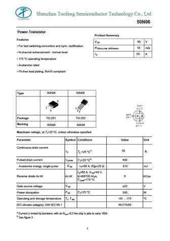
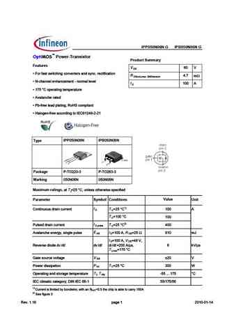
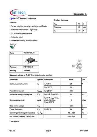
Shenzhen Tuofeng Semiconductor Technology Co., Ltd 50N06 Power-Transistor Product Summary Features V 60 V DS For fast switching converters and sync. rectification R 15 m DS(on),max SMDversion N-channel enhancement - normal level I 50 A D 175 C operating temperature Avalanche rated Pb-free lead plating, RoHS compliant 50N06 Type 50N06 2 1 1 3 2 3... See More ⇒
50n06.pdf
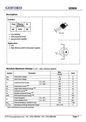
GOFORD 50N06 Description Features VDSS RDS(ON) ID VDSS RDS(ON) ID @ (typ) @ 10V (typ) 10V 19m 50A 60V 60V 19m 50A Fast switching 100% avalanche tested Improved dv/dt capability Application UPS High efficiency switch mode power supplies Absolute Maximum Ratings TC=25 unless otherwise specified Max. Symbol Parameter Units TO-... See More ⇒
50n06 f50n06 i50n06 e50n06 b50n06 d50n06.pdf
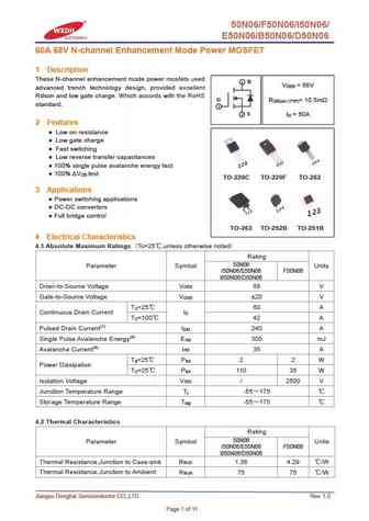
50N06/F50N06/I50N06/ E50N06/B50N06/D50N06 60A 68V N-channel Enhancement Mode Power MOSFET 1 Description These N-channel enhancement mode power mosfets used 2 D V = 68V DSS advanced trench technology design, provided excellent Rdson and low gate charge. Which accords with the RoHS G R = 10.5m DS(on) (TYP) standard. 1 3 S I = 60A D 2 Features Low on resistance Low ga... See More ⇒
50n06.pdf
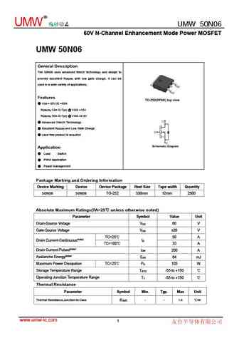
R UMW UMW 50N06 60V N-Channel Enhancement Mode Power MOSFET UMW 50N06 General Description The 50N06 uses advanced trench technology and design to provide excellent RDS(ON) with low gate charge. It can be used in a wide variety of applications. Features VDS = 60V,ID =50A RDS(ON),12m (Typ) @ VGS =10V RDS(ON),16m (Typ) @ VGS =4.5V Advanced Trench Technology Excellent RDS(ON) and L... See More ⇒
50n06.pdf
50N06 60V N-Channel Enhancement Mode Power MOSFET 50N06 General Description The 50N06 uses advanced trench technology and design to provide excellent RDS(ON) with low gate charge. It can be used in a wide variety of applications. Features VDS = 60V,ID =50A RDS(ON),12m (Typ) @ VGS =10V RDS(ON),16m (Typ) @ VGS =4.5V Advanced Trench Technology Excellent RDS(ON) and Low Gate Charge ... See More ⇒
50n06.pdf
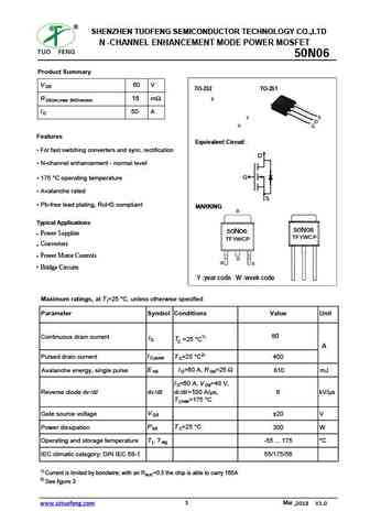
SHENZHEN TUOFENG SEMICONDUCTOR TECHNOLOGY CO.,LTD N -CHANNEL ENHANCEMENT MODE POWER MOSFET 50N06 Product Summary V 60 V DS TO-252 TO-251 R 15 m D DS(on),max SMDversion I 50 A D S S D G G Features Equivalent Circuit For fast switching converters and sync. rectification D N-channel enhancement - normal level G 175 C operating temperature Avalanche... See More ⇒
50n06 50n06f 50n06b 50n06h 50n06g 50n06d.pdf
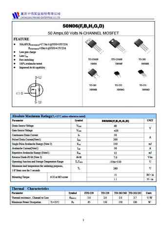
50N06(F,B,H,G,D) 50 Amps,60 Volts N-CHANNEL MOSFET FEATURE 50A,60V,R =17.5m @VGS=10V/25A DS(ON)MAX R =20m @VGS=4.5V/25A DS(ON)MAX Low gate charge Low C iss TO-220AB ITO-220AB TO-262 Fast switching 100% avalanche tested 50N06 50N06F 50N06H Improved dv/dt capability TO-263 TO-252 TO-251 50N06B 50N06G 50N06D Absolute Maximum Ratings(T =25 ,unless otherwi... See More ⇒
tsp50n06m tsf50n06m.pdf
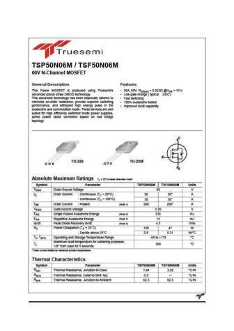
TSP50N06M / TSF50N06M 60V N-Channel MOSFET General Description Features This Power MOSFET is produced using Truesemi s 50A, 60V, RDS(on) = 0.023 @VGS = 10 V advanced planar stripe DMOS technology. Low gate charge ( typical 33nC) This advanced technology has been especially tailored to Fast switching minimize on-state resistance, provide superior switching 100% avala... See More ⇒
kia50n06.pdf

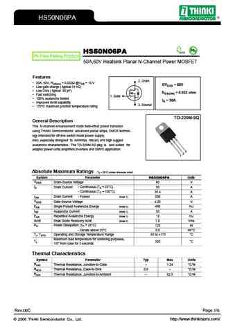
KIA50N06 Pb KIA50N06 Pb Free Plating Product 50A,60V Heatsink Planar N-Channel Power MOSFET Features 2. Drain 50A, 60V, RDS(on) = 0.022 @VGS = 10 V BVDSS = 60V Low gate charge ( typical 31 nC) Low Crss ( typical 65 pF) RDS(ON) = 0.022 ohm Fast switching 1. Gate 100% avalanche tested ID = 50A ... See More ⇒
ipd50n06s2l-13.pdf
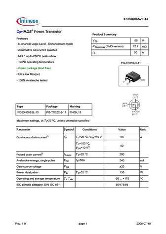
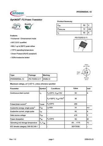
IPD50N06S2L-13 OptiMOS Power-Transistor Product Summary Features V 55 V DS N-channel Logic Level - Enhancement mode R (SMD version) 12.7 m DS(on),max Automotive AEC Q101 qualified I 50 A D MSL1 up to 260 C peak reflow 175 C operating temperature PG-TO252-3-11 Green package (lead free) Ultra low Rds(on) 100% Avalanche tested Type Package Mark... See More ⇒
mcac50n06y-tp.pdf
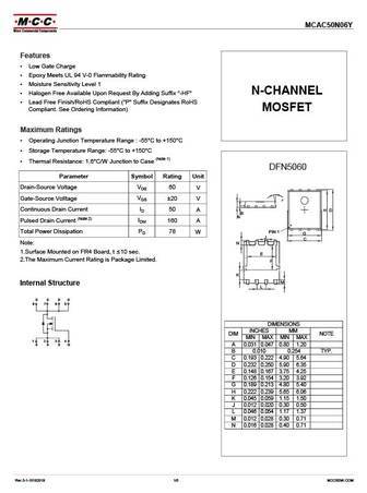
MCAC50N06Y Electrical Characteristics @ 25 C (Unless Otherwise Specified) Parameter Symbol Test Conditions Min Typ Max Unit Static Characteristics V(BR)DSS VGS=0V, ID=250 A Drain-Source Breakdown Voltage 60 V IGSS VDS=0V, VGS = 20V Gate-Source Leakage Current 100 nA IDSS VDS=48V, VGS=0V, TJ=25 C Zero Gate Voltage Drain Current 1 A VGS(th) VDS=VGS, ID=250 A Gate-Threshol... See More ⇒
ste250n06.pdf
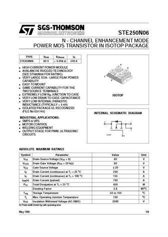
STE250N06 N - CHANNEL ENHANCEMENT MODE POWER MOS TRANSISTOR IN ISOTOP PACKAGE TYPE VDSS RDS(on) ID STE250N06 60 V ... See More ⇒
mtb50n06vrev3.pdf

MOTOROLA Order this document SEMICONDUCTOR TECHNICAL DATA by MTB50N06V/D Designer's Data Sheet MTB50N06V TMOS V Motorola Preferred Device Power Field Effect Transistor D2PAK for Surface Mount TMOS POWER FET N Channel Enhancement Mode Silicon Gate 42 AMPERES 60 VOLTS TMOS V is a new technology designed to achieve an on resistance RDS(on) = 0.028 OHM area product about ... See More ⇒
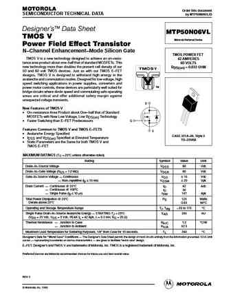
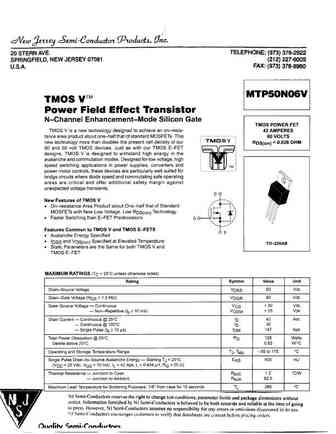
mtp50n06v.pdf

MOTOROLA Order this document SEMICONDUCTOR TECHNICAL DATA by MTP50N06V/D Designer's Data Sheet MTP50N06V TMOS V Motorola Preferred Device Power Field Effect Transistor N Channel Enhancement Mode Silicon Gate TMOS POWER FET TMOS V is a new technology designed to achieve an on resis- 42 AMPERES tance area product about one half that of standard MOSFETs. This 60 VOL... See More ⇒
mtb50n06el.pdf

MOTOROLA Order this document SEMICONDUCTOR TECHNICAL DATA by MTB50N06EL/D Advance Information MTB50N06EL TMOS E-FET. Motorola Preferred Device Power Field Effect Transistors TMOS POWER FET D2PAK for Surface Mount LOGIC LEVEL Logic Level TMOS (L2TMOS ) 50 AMPERES 60 VOLTS N Channel Enhancement Mode Silicon Gate RDS(on) = 0.028 OHM These TMOS Power FETs are designed fo... See More ⇒
mtp50n06el.pdf
MOTOROLA Order this document SEMICONDUCTOR TECHNICAL DATA by MTP50N06EL/D Designer's Data Sheet MTP50N06EL TMOS E-FET. Motorola Preferred Device Power Field Effect Transistor N Channel Enhancement Mode Silicon Gate TMOS POWER FET This advanced TMOS E FET is designed to withstand high 50 AMPERES energy in the avalanche and commutation modes. The new energy 60 VOLTS eff... See More ⇒
mtp50n06vrev3.pdf
MOTOROLA Order this document SEMICONDUCTOR TECHNICAL DATA by MTP50N06V/D Designer's Data Sheet MTP50N06V TMOS V Motorola Preferred Device Power Field Effect Transistor N Channel Enhancement Mode Silicon Gate TMOS POWER FET TMOS V is a new technology designed to achieve an on resis- 42 AMPERES tance area product about one half that of standard MOSFETs. This 60 VOL... See More ⇒
mtb50n06vl.pdf

MOTOROLA Order this document SEMICONDUCTOR TECHNICAL DATA by MTB50N06VL/D Designer's Data Sheet MTB50N06VL TMOS V Motorola Preferred Device Power Field Effect Transistor D2PAK for Surface Mount TMOS POWER FET N Channel Enhancement Mode Silicon Gate 42 AMPERES 60 VOLTS TMOS V is a new technology designed to achieve an on resistance RDS(on) = 0.032 OHM area product abou... See More ⇒
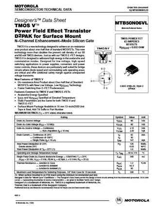
mtb50n06v.pdf
MOTOROLA Order this document SEMICONDUCTOR TECHNICAL DATA by MTB50N06V/D Designer's Data Sheet MTB50N06V TMOS V Motorola Preferred Device Power Field Effect Transistor D2PAK for Surface Mount TMOS POWER FET N Channel Enhancement Mode Silicon Gate 42 AMPERES 60 VOLTS TMOS V is a new technology designed to achieve an on resistance RDS(on) = 0.028 OHM area product about ... See More ⇒
mtb50n06elrev1.pdf
MOTOROLA Order this document SEMICONDUCTOR TECHNICAL DATA by MTB50N06EL/D Advance Information MTB50N06EL TMOS E-FET. Motorola Preferred Device Power Field Effect Transistors TMOS POWER FET D2PAK for Surface Mount LOGIC LEVEL Logic Level TMOS (L2TMOS ) 50 AMPERES 60 VOLTS N Channel Enhancement Mode Silicon Gate RDS(on) = 0.028 OHM These TMOS Power FETs are designed fo... See More ⇒
mtp50n06vl.pdf
MOTOROLA Order this document SEMICONDUCTOR TECHNICAL DATA by MTP50N06VL/D Designer's Data Sheet MTP50N06VL TMOS V Motorola Preferred Device Power Field Effect Transistor N Channel Enhancement Mode Silicon Gate TMOS POWER FET TMOS V is a new technology designed to achieve an on resis- 42 AMPERES tance area product about one half that of standard MOSFETs. This 60 VOLTS ... See More ⇒
mtb50n06vlrev2.pdf
MOTOROLA Order this document SEMICONDUCTOR TECHNICAL DATA by MTB50N06VL/D Designer's Data Sheet MTB50N06VL TMOS V Motorola Preferred Device Power Field Effect Transistor D2PAK for Surface Mount TMOS POWER FET N Channel Enhancement Mode Silicon Gate 42 AMPERES 60 VOLTS TMOS V is a new technology designed to achieve an on resistance RDS(on) = 0.032 OHM area product abou... See More ⇒
phd50n06lt.pdf

Philips Semiconductors Product specification TrenchMOS transistor PHP50N06LT, PHB50N06LT, PHD50N06LT Logic level FET FEATURES SYMBOL QUICK REFERENCE DATA Trench technology VDSS = 55 V d Very low on-state resistance Fast switching ID = 50 A Stable off-state characteristics High thermal cycling performance RDS(ON) 24 m (VGS = 5 V) g Low thermal... See More ⇒
php50n06lt 3.pdf
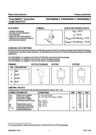
Philips Semiconductors Product specification TrenchMOS transistor PHP50N06LT, PHB50N06LT, PHD50N06LT Logic level FET FEATURES SYMBOL QUICK REFERENCE DATA Trench technology VDSS = 55 V d Very low on-state resistance Fast switching ID = 50 A Stable off-state characteristics High thermal cycling performance RDS(ON) 24 m (VGS = 5 V) g Low thermal... See More ⇒
phb50n06t 1.pdf
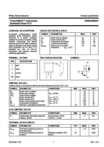
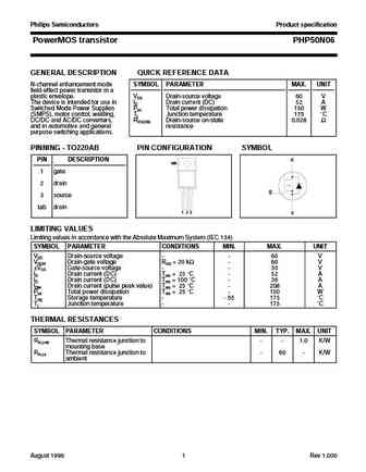
Philips Semiconductors Product specification TrenchMOS transistor PHB50N06T Standard level FET GENERAL DESCRIPTION QUICK REFERENCE DATA N-channel enhancement mode SYMBOL PARAMETER MAX. UNIT standard level field-effect power transistor in a plastic envelope VDS Drain-source voltage 55 V suitable for surface mounting. Using ID Drain current (DC) 50 A trench technology the devic... See More ⇒
php50n06 1.pdf
Philips Semiconductors Product specification PowerMOS transistor PHP50N06 GENERAL DESCRIPTION QUICK REFERENCE DATA N-channel enhancement mode SYMBOL PARAMETER MAX. UNIT field-effect power transistor in a plastic envelope. VDS Drain-source voltage 60 V The device is intended for use in ID Drain current (DC) 52 A Switched Mode Power Supplies Ptot Total power dissipation 150 W (SMPS), mo... See More ⇒
phb50n06lt.pdf
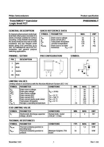
Philips Semiconductors Product specification TrenchMOS transistor PHB50N06LT Logic level FET GENERAL DESCRIPTION QUICK REFERENCE DATA N-channel enhancement mode logic SYMBOL PARAMETER MAX. UNIT level field-effect power transistor in a plastic envelope suitable for surface VDS Drain-source voltage 55 V mounting. Using trench technology ID Drain current (DC) 50 A the device fea... See More ⇒
stp50n06l.pdf

STP50N06L STP50N06LFI N - CHANNEL ENHANCEMENT MODE LOW THRESHOLD POWER MOS TRANSISTOR TYPE VDSS RDS(on) ID STP50N06L 60 V ... See More ⇒
stp50n06-.pdf
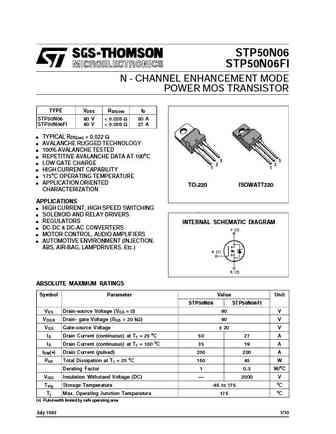
STP50N06 STP50N06FI N - CHANNEL ENHANCEMENT MODE POWER MOS TRANSISTOR TYPE V R I DSS DS(on) D STP50N06 60 V ... See More ⇒
stp50n06.pdf
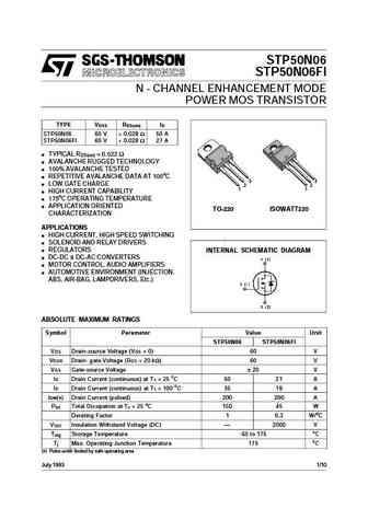
STP50N06 STP50N06FI N - CHANNEL ENHANCEMENT MODE POWER MOS TRANSISTOR TYPE VDSS RDS(on) ID STP50N06 60 V ... See More ⇒
stp50n06l-fi.pdf
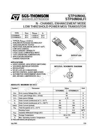
STP50N06L STP50N06LFI N - CHANNEL ENHANCEMENT MODE LOW THRESHOLD POWER MOS TRANSISTOR TYPE VDSS RDS(on) ID STP50N06L 60 V ... See More ⇒
rfg50n06 rfp50n06 rf1s50n06sm.pdf
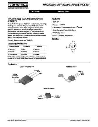
RFG50N06, RFP50N06, RF1S50N06SM Data Sheet January 2002 50A, 60V, 0.022 Ohm, N-Channel Power Features MOSFETs 50A, 60V These N-Channel power MOSFETs are manufactured using rDS(ON) = 0.022 the MegaFET process. This process, which uses feature Temperature Compensating PSPICE Model sizes approaching those of LSI integrated circuits gives optimum utilization of silico... See More ⇒
fqb50n06 fqi50n06.pdf

October 2008 QFET FQB50N06 / FQI50N06 60V N-Channel MOSFET General Description Features These N-Channel enhancement mode power field effect 50A, 60V, RDS(on) = 0.022 @VGS = 10 V transistors are produced using Fairchild s proprietary, Low gate charge ( typical 31 nC) planar stripe, DMOS technology. Low Crss ( typical 65 pF) This advanced technology has been especially... See More ⇒
fqp50n06.pdf

TM QFET FQP50N06 60V N-Channel MOSFET General Description Features These N-Channel enhancement mode power field effect 50A, 60V, RDS(on) = 0.022 @VGS = 10 V transistors are produced using Fairchild s proprietary, Low gate charge ( typical 31 nC) planar stripe, DMOS technology. Low Crss ( typical 65 pF) This advanced technology has been especially tailored to Fast ... See More ⇒
fqb50n06tm fqi50n06tu.pdf
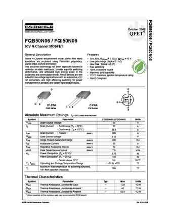
October 2008 QFET FQB50N06 / FQI50N06 60V N-Channel MOSFET General Description Features These N-Channel enhancement mode power field effect 50A, 60V, RDS(on) = 0.022 @VGS = 10 V transistors are produced using Fairchild s proprietary, Low gate charge ( typical 31 nC) planar stripe, DMOS technology. Low Crss ( typical 65 pF) This advanced technology has been especially... See More ⇒
fqpf50n06l.pdf
May 2001 TM QFET FQPF50N06L 60V LOGIC N-Channel MOSFET General Description Features These N-Channel enhancement mode power field effect 32.6A, 60V, RDS(on) = 0.021 @VGS = 10 V transistors are produced using Fairchild s proprietary, Low gate charge ( typical 24.5 nC) planar stripe, DMOS technology. Low Crss ( typical 90 pF) This advanced technology has been especially ... See More ⇒
fqb50n06ltm fqi50n06ltu.pdf
October 2008 QFET FQB50N06L / FQI50N06L 60V LOGIC N-Channel MOSFET General Description Features These N-Channel enhancement mode power field effect 52.4A, 60V, RDS(on) = 0.021 @VGS = 10 V transistors are produced using Fairchild s proprietary, Low gate charge ( typical 24.5 nC) planar stripe, DMOS technology. Low Crss ( typical 90 pF) This advanced technology has bee... See More ⇒
fqpf50n06.pdf
May 2001 TM QFET FQPF50N06 60V N-Channel MOSFET General Description Features These N-Channel enhancement mode power field effect 31A, 60V, RDS(on) = 0.022 @VGS = 10 V transistors are produced using Fairchild s proprietary, Low gate charge ( typical 31 nC) planar stripe, DMOS technology. Low Crss ( typical 65 pF) This advanced technology has been especially tailored to... See More ⇒
fqb50n06l fqi50n06l.pdf

October 2008 QFET FQB50N06L / FQI50N06L 60V LOGIC N-Channel MOSFET General Description Features These N-Channel enhancement mode power field effect 52.4A, 60V, RDS(on) = 0.021 @VGS = 10 V transistors are produced using Fairchild s proprietary, Low gate charge ( typical 24.5 nC) planar stripe, DMOS technology. Low Crss ( typical 90 pF) This advanced technology has bee... See More ⇒
fqp50n06l.pdf
May 2001 TM QFET FQP50N06L 60V LOGIC N-Channel MOSFET General Description Features These N-Channel enhancement mode power field effect 52.4A, 60V, RDS(on) = 0.021 @VGS = 10 V transistors are produced using Fairchild s proprietary, Low gate charge ( typical 24.5 nC) planar stripe, DMOS technology. Low Crss ( typical 90 pF) This advanced technology has been especially t... See More ⇒
rsd050n06fra.pdf

Data Sheet AEC-Q101 Qualified 4V Drive Nch MOSFET RSD050N06FRA Structure Dimensions (Unit mm) Silicon N-channel MOSFET CPT3 (SC-63) Features 1) Low on-resistance. 2) Fast switching speed. 3) Drive circuits can be simple. 9 3) Parallel use is easy. Applications Switching Packaging specif... See More ⇒
rsd050n06.pdf
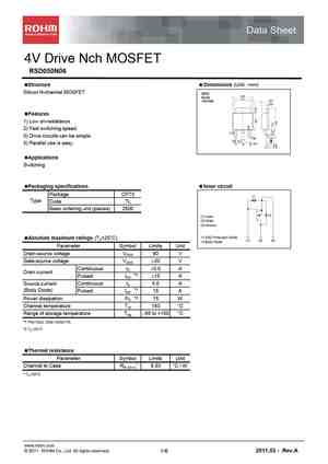
Data Sheet 4V Drive Nch MOSFET RSD050N06 Structure Dimensions (Unit mm) Silicon N-channel MOSFET CPT3 (SC-63) Features 1) Low on-resistance. 2) Fast switching speed. 3) Drive circuits can be simple. 9 3) Parallel use is easy. Applications Switching Packaging specifications Inner circ... See More ⇒
rsd150n06.pdf

Data Sheet 4V Drive Nch MOSFET RSD150N06 Structure Dimensions (Unit mm) Silicon N-channel MOSFET CPT3 (SC-63) Features 1) Low on-resistance. 2) Fast switching speed. 3) Drive circuits can be simple. 9 4) Parallel use is easy. Applications Switching Packaging specifications Inner ci... See More ⇒
rsd050n06tl.pdf

Data Sheet 4V Drive Nch MOSFET RSD050N06 Structure Dimensions (Unit mm) Silicon N-channel MOSFET CPT3 (SC-63) Features 1) Low on-resistance. 2) Fast switching speed. 3) Drive circuits can be simple. 9 3) Parallel use is easy. Applications Switching Packaging specifications Inner circ... See More ⇒
rsd150n06fra.pdf
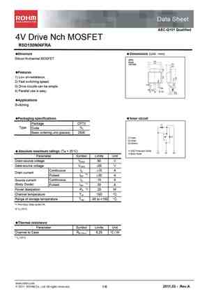
Data Sheet AEC-Q101 Qualified 4V Drive Nch MOSFET RSD150N06FRA Structure Dimensions (Unit mm) Silicon N-channel MOSFET CPT3 (SC-63) Features 1) Low on-resistance. 2) Fast switching speed. 3) Drive circuits can be simple. 9 4) Parallel use is easy. Applications Switching Packaging spec... See More ⇒
sum50n06-16l.pdf
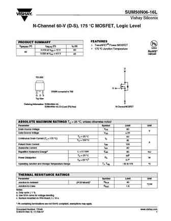
SUM50N06-16L Vishay Siliconix N-Channel 60-V (D-S), 175 C MOSFET, Logic Level FEATURES PRODUCT SUMMARY TrenchFET Power MOSFET V(BR)DSS (V) rDS(on) ( )ID (A) Available 175 C Junction Temperature 0.016 at VGS = 10 V 50 RoHS* 60 0.022 at VGS = 4.5 V 43 COMPLIANT D TO-263 G DRAIN connected to TAB G D S Top View S Ordering Information SUM50N06-16L SUM50N06-1... See More ⇒
sud50n06-07l.pdf
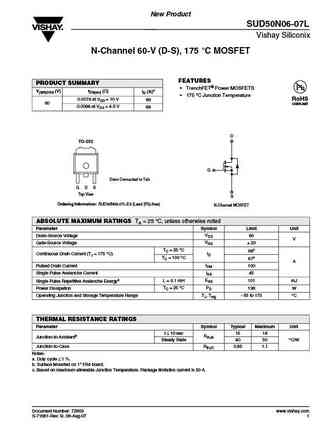
New Product SUD50N06-07L Vishay Siliconix N-Channel 60-V (D-S), 175 C MOSFET FEATURES PRODUCT SUMMARY TrenchFET Power MOSFETS V(BR)DSS (V) rDS(on) ( ) ID (A)c 175 C Junction Temperature 0.0074 at VGS = 10 V RoHS 96 60 COMPLIANT 0.0088 at VGS = 4.5 V 88 D TO-252 G Drain Connected to Tab G D S Top View S Ordering Information SUD50N06-07L-E3 (Lead (Pb)-... See More ⇒
sqp50n06-09l.pdf
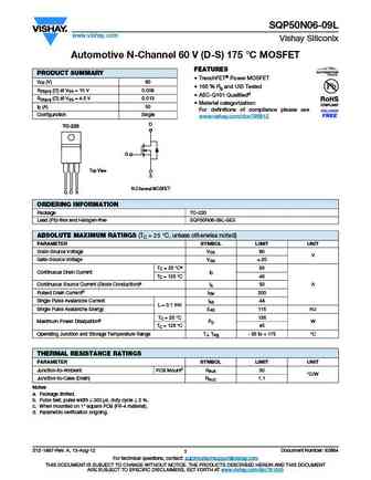
SQP50N06-09L www.vishay.com Vishay Siliconix Automotive N-Channel 60 V (D-S) 175 C MOSFET FEATURES PRODUCT SUMMARY TrenchFET Power MOSFET VDS (V) 60 100 % Rg and UIS Tested RDS(on) ( ) at VGS = 10 V 0.009 AEC-Q101 Qualifiedd RDS(on) ( ) at VGS = 4.5 V 0.013 Material categorization ID (A) 50 For definitions of compliance please see Configuration Single ww... See More ⇒
sqr50n06-07l.pdf
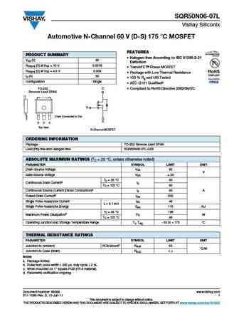
SQR50N06-07L Vishay Siliconix Automotive N-Channel 60 V (D-S) 175 C MOSFET FEATURES PRODUCT SUMMARY Halogen-free According to IEC 61249-2-21 VDS (V) 60 Definition RDS(on) ( ) at VGS = 10 V 0.0076 TrenchFET Power MOSFET RDS(on) ( ) at VGS = 4.5 V 0.009 Package with Low Thermal Resistance ID (A) 50 100 % Rg and UIS Tested Configuration Single AEC-Q101 Qu... See More ⇒
sud50n06-08h.pdf
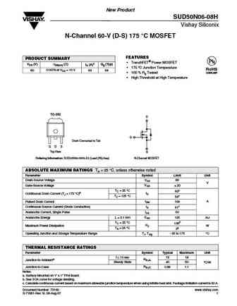
New Product SUD50N06-08H Vishay Siliconix N-Channel 60-V (D-S) 175 C MOSFET FEATURES PRODUCT SUMMARY TrenchFET Power MOSFET VDS (V) rDS(on) ( ) ID (A)c Qg (Typ) 175 C Junction Temperature 0.0078 at VGS = 10 V RoHS 60 93 94 100 % Rg Tested COMPLIANT High Threshold at High Temperature TO-252 D G Drain Connected to Tab G D S Top View S Ordering In... See More ⇒
sud50n06.pdf
SUD50N06-09L Vishay Siliconix N-Channel 60 V (D-S), 175 C MOSFET, Logic Level FEATURES PRODUCT SUMMARY TrenchFET Power MOSFET VDS (V) rDS(on) ( ) ID (A)a Available 175 C Junction Temperature 0.0093 at VGS = 10 V 50 RoHS* 60 0.0122 at VGS = 4.5 V 50 COMPLIANT TO-252 D G Drain Connected to Tab G D S Top View S Ordering Information SUD50N06-09L SUD50N06... See More ⇒
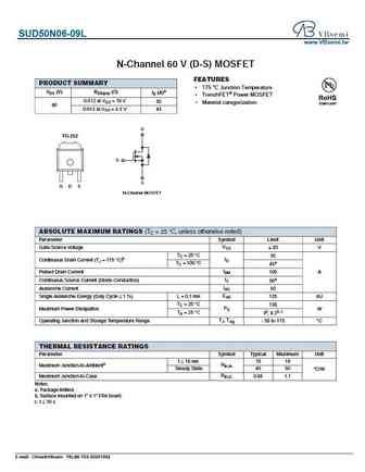
sud50n06-09l.pdf
SUD50N06-09L Vishay Siliconix N-Channel 60 V (D-S), 175 C MOSFET, Logic Level FEATURES PRODUCT SUMMARY 175 C Junction Temperature VDS (V) RDS(on) ( ) ID (A)a TrenchFET Power MOSFET 0.0093 at VGS = 10 V 50 Material categorization 60 0.0122 at VGS = 4.5 V 50 For definitions of compliance please see www.vishay.com/doc?99912 TO-252 D G Drain Connected ... See More ⇒
sqd50n06-07l.pdf
SQD50N06-07L www.vishay.com Vishay Siliconix Automotive N-Channel 60 V (D-S) 175 C MOSFET FEATURES PRODUCT SUMMARY Halogen-free According to IEC 61249-2-21 VDS (V) 60 Definition RDS(on) ( ) at VGS = 10 V 0.0076 TrenchFET Power MOSFET RDS(on) ( ) at VGS = 4.5 V 0.009 Package with Low Thermal Resistance ID (A) 50 100 % Rg and UIS Tested Configuration Single ... See More ⇒
sqd50n06-09l.pdf
SQD50N06-09L www.vishay.com Vishay Siliconix Automotive N-Channel 60 V (D-S) 175 C MOSFET FEATURES PRODUCT SUMMARY Halogen-free According to IEC 61249-2-21 VDS (V) 60 Definition RDS(on) ( ) at VGS = 10 V 0.009 TrenchFET Power MOSFET RDS(on) ( ) at VGS = 4.5 V 0.013 100 % Rg and UIS Tested ID (A) 50 Compliant to RoHS Directive 2002/95/EC Configuration Singl... See More ⇒
spd50n06s2-14.pdf
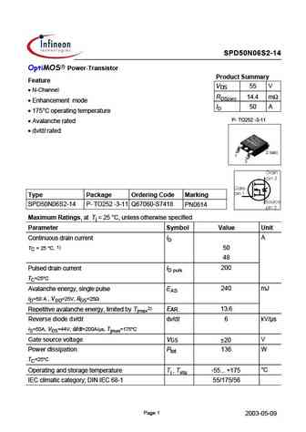
SPD50N06S2-14 OptiMOS Power-Transistor Product Summary Feature VDS 55 V N-Channel RDS(on) 14.4 m Enhancement mode ID 50 A 175 C operating temperature P- TO252 -3-11 Avalanche rated dv/dt rated Type Package Ordering Code Marking SPD50N06S2-14 P- TO252 -3-11 Q67060-S7418 PN0614 Maximum Ratings, at Tj = 25 C, unless otherwise specified Parameter Symbo... See More ⇒
ipd50n06s4l-08 ipd50n06s4l-08 ds 10.pdf
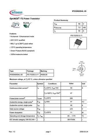
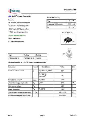
IPD50N06S4L-08 OptiMOS -T2 Power-Transistor Product Summary V 60 V DS R 7.8 m DS(on),max I 50 A D Features PG-TO252-3-11 N-channel - Enhancement mode AEC Q101 qualified MSL1 up to 260 C peak reflow 175 C operating temperature Green Product (RoHS compliant) 100% Avalanche tested Type Package Marking IPD50N06S4L-08 PG-TO252-3-11 4N06L08 Maximum ra... See More ⇒
ipd250n06n3.pdf
pe # ! ! # A03 B53 R m D n) m x Q ( @D9=9J54 D538>?F5BD5BC I D Q H35>5?B=1... See More ⇒
ipd50n06s2l-13.pdf
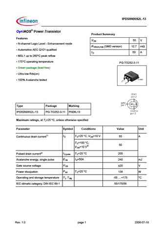
IPD50N06S2L-13 OptiMOS Power-Transistor Product Summary Features V 55 V DS N-channel Logic Level - Enhancement mode R (SMD version) 12.7 m DS(on),max Automotive AEC Q101 qualified I 50 A D MSL1 up to 260 C peak reflow 175 C operating temperature PG-TO252-3-11 Green package (lead free) Ultra low Rds(on) 100% Avalanche tested Type Package Mark... See More ⇒
ipb050n06ng ipp050n06ng.pdf
IPP050N06N G IPB050N06N G Power-Transistor Product Summary Features V D O >@ 50AB AE8B278=6 2>=D4@B4@A 0=3 AG=2 @42B85820B8>= R 4 7 m + >= = O ' 270==4; 4=70=24@?4@0B8=6 B4"+ 2>64= 5@44 022>@38=6 B> # Type #)) ' ' #) ' ' Package O O Mar... See More ⇒
ipd50n06s2-14 ipd50n06s2-14 ds 1 1.pdf
IPD50N06S2-14 Power-Transistor Product Summary Features V 55 V DS N-channel - Enhancement mode R (SMD version) 14.4 m DS(on),max Automotive AEC Q101 qualified I 50 A D MSL1 up to 260 C peak reflow 175 C operating temperature PG-TO252-3-11 Green package (lead free) Ultra low Rds(on) 100% Avalanche tested Type Package Marking IPD50N06S2-14... See More ⇒
ipd50n06s4-09 ipd50n06s4-09 ds 12.pdf

IPD50N06S4-09 OptiMOS -T2 Power-Transistor Product Summary V 60 V DS R 9.0 m DS(on),max I 50 A D Features PG-TO252-3-11 N-channel - Enhancement mode AEC qualified MSL1 up to 260 C peak reflow 175 C operating temperature Green Product (RoHS compliant) 100% Avalanche tested Type Package Marking IPD50N06S4-09 PG-TO252-3-11 4N0609 Maximum ratings, a... See More ⇒
ipd350n06lg.pdf
% # ! % (>.;?6?@ %>E Features D P ?A 61BC BF9C389>7 3?>E5AC5AB 1>4 BH>3 A53C96931C9?> mW D n) m x P ( 381>>581>35=5>C ... See More ⇒
ipd50n06s4l-12 ipd50n06s4l-12 ds 10.pdf
IPD50N06S4L-12 OptiMOS -T2 Power-Transistor Product Summary V 60 V DS R 12 m DS(on),max I 50 A D Features PG-TO252-3-11 N-channel - Enhancement mode AEC Q101 qualified MSL1 up to 260 C peak reflow 175 C operating temperature Green Product (RoHS compliant) 100% Avalanche tested Type Package Marking IPD50N06S4L-12 PG-TO252-3-11 4N06L12 Maximum rat... See More ⇒
ixtq150n06p.pdf
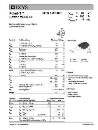
IXTQ 150N06P VDSS = 60 V PolarHTTM ID25 = 150 A Power MOSFET RDS(on) 10 m N-Channel Enhancement Mode Avalanche Rated Symbol Test Conditions Maximum Ratings TO-3P (IXTQ) VDSS TJ = 25 C to 175 C60 V VDGR TJ = 25 C to 175 C; RGS = 1 M 60 V VGS Continuous 20 V G VGSM Transient 30 V D (TAB) S ID25 TC = 25 C 150 A IDRMS Ext... See More ⇒
mcac50n06y.pdf
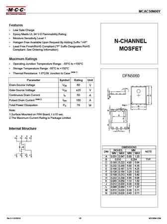
MCAC50N06Y Electrical Characteristics @ 25 C (Unless Otherwise Specified) Parameter Symbol Test Conditions Min Typ Max Unit Static Characteristics V(BR)DSS VGS=0V, ID=250 A Drain-Source Breakdown Voltage 60 V IGSS VDS=0V, VGS = 20V Gate-Source Leakage Current 100 nA IDSS VDS=48V, VGS=0V, TJ=25 C Zero Gate Voltage Drain Current 1 A VGS(th) VDS=VGS, ID=250 A Gate-Threshol... See More ⇒
oms150n06f.pdf
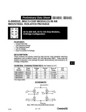
OMS150N06FL OMS60L60FL Preliminary Data Sheet OMS120N10FL OMS50F60FL H-BRIDGE, MULTI-CHIP MODULES IN AN INDUSTRIAL ISOLATED PACKAGE 60 To 600 Volt, 50 To 150 Amp Modules, H-Bridge Configuration FEATURES Isolated Heat Sink Low Inductance Design Fast Switching Speed Low On Voltage Easy-To-Connect To Package DESCRIPTION These modules are ideally suited for high d... See More ⇒
fqb50n06 fqi50n06.pdf

Is Now Part of To learn more about ON Semiconductor, please visit our website at www.onsemi.com Please note As part of the Fairchild Semiconductor integration, some of the Fairchild orderable part numbers will need to change in order to meet ON Semiconductor s system requirements. Since the ON Semiconductor product management systems do not have the ability to manage part nomenclatur... See More ⇒
fqp50n06.pdf
TM QFET FQP50N06 60V N-Channel MOSFET General Description Features These N-Channel enhancement mode power field effect 50A, 60V, RDS(on) = 0.022 @VGS = 10 V transistors are produced using Fairchild s proprietary, Low gate charge ( typical 31 nC) planar stripe, DMOS technology. Low Crss ( typical 65 pF) This advanced technology has been especially tailored to Fast ... See More ⇒
utc50n06l.pdf
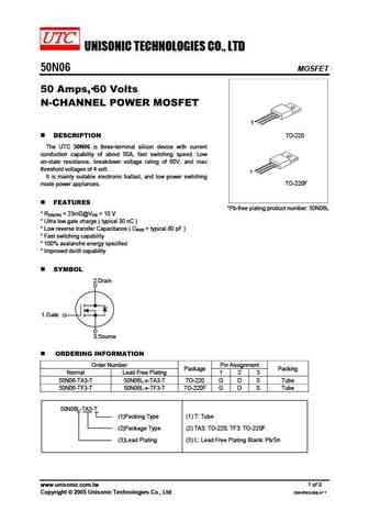
UNISONIC TECHNOLOGIES CO., LTD 50N06 MOSFET 50 Amps, 60 Volts N-CHANNEL POWER MOSFET 1 DESCRIPTION TO-220 The UTC 50N06 is three-terminal silicon device with current conduction capability of about 50A, fast switching speed. Low on-state resistance, breakdown voltage rating of 60V, and max threshold voltages of 4 volt. 1 It is mainly suitable electronic ballast, and low po... See More ⇒
utt150n06.pdf
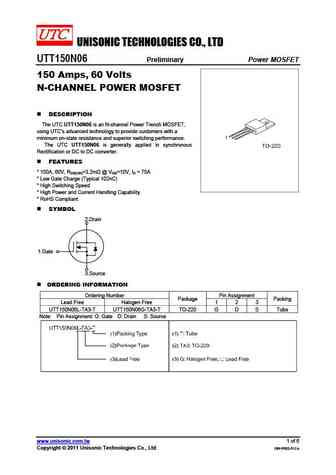
UNISONIC TECHNOLOGIES CO., LTD UTT150N06 Preliminary Power MOSFET 150 Amps, 60 Volts N-CHANNEL POWER MOSFET DESCRIPTION The UTC UTT150N06 is an N-channel Power Trench MOSFET, using UTC s advanced technology to provide customers with a minimum on-state resistance and superior switching performance. The UTC UTT150N06 is generally applied in synchronous Rectification or DC t... See More ⇒
utt50n06.pdf
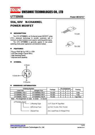
UNISONIC TECHNOLOGIES CO., LTD UTT50N06 Power MOSFET 50A, 60V N-CHANNEL POWER MOSFET DESCRIPTION The UTC UTT50N06 is an N-channel power MOSFET using UTC s advanced technology to provide customers with a minimum on-state resistance and superior switching performance. The UTC UTT50N06 is generally applied in low power switching mode power appliances and electronic ballast. ... See More ⇒
50n06l-ta3-t 50n06g-ta3-t 50n06l-tf3-t 50n06g-tf3-t 50n06l-tf3t-t 50n06g-tf3t-t 50n60l-tm3-t 50n60g-tm3-t.pdf

UNISONIC TECHNOLOGIES CO., LTD 50N06 Power MOSFET 50 Amps, 60 Volts N-CHANNEL POWER MOSFET 1 1 DESCRIPTION TO-263 TO-251 The UTC 50N06 is three-terminal silicon device with current conduction capability of about 50A, fast switching speed. Low on-state resistance, breakdown voltage rating of 60V, and max threshold voltages of 4 volt. 1 1 It is mainly suitable electronic ... See More ⇒
50n06l-tn3-r 50n06g-tn3-r 50n06l-tnd-r 50n06g-tnd-r 50n06l-tq2-t 50n06g-tq2-t 50n06l-tq2-r 50n06g-tq2-r.pdf
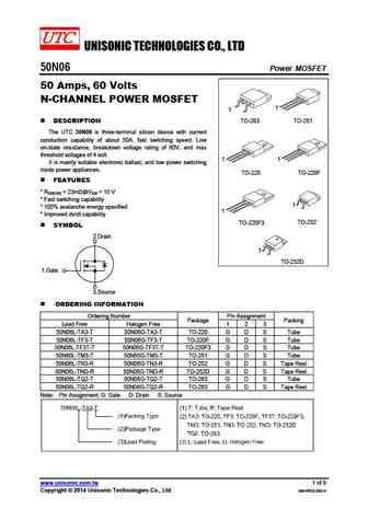
UNISONIC TECHNOLOGIES CO., LTD 50N06 Power MOSFET 50 Amps, 60 Volts N-CHANNEL POWER MOSFET 1 1 DESCRIPTION TO-263 TO-251 The UTC 50N06 is three-terminal silicon device with current conduction capability of about 50A, fast switching speed. Low on-state resistance, breakdown voltage rating of 60V, and max threshold voltages of 4 volt. 1 1 It is mainly suitable electronic ... See More ⇒
rfp50n06.pdf
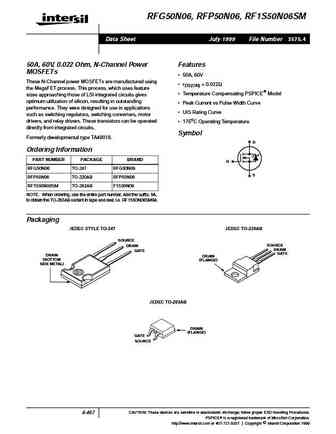
RFG50N06, RFP50N06, RF1S50N06SM Data Sheet July 1999 File Number 3575.4 50A, 60V, 0.022 Ohm, N-Channel Power Features MOSFETs 50A, 60V These N-Channel power MOSFETs are manufactured using rDS(ON) = 0.022 the MegaFET process. This process, which uses feature Temperature Compensating PSPICE Model sizes approaching those of LSI integrated circuits gives optimum utilizati... See More ⇒
rfg50n06le rfp50n06le rf1s50n06lesm.pdf
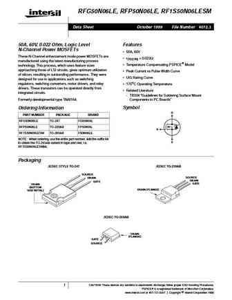
RFG50N06LE, RFP50N06LE, RF1S50N06LESM Data Sheet October 1999 File Number 4072.3 50A, 60V, 0.022 Ohm, Logic Level Features N-Channel Power MOSFETs 50A, 60V These N-Channel enhancement mode power MOSFETs are rDS(ON) = 0.022 manufactured using the latest manufacturing process Temperature Compensating PSPICE Model technology. This process, which uses feature sizes approa... See More ⇒
ssd50n06-15d.pdf
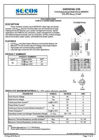
SSD50N06-15D N-Ch Enhancement Mode Power MOSFET 51A, 60V, RDS(ON) 13 m Elektronische Bauelemente RoHS Compliant Product A suffix of -C specifies halogen & lead-free TO-252(D-Pack) DESCRIPTION These miniature surface mount MOSFETs utilize high cell density process. Low RDS(on) assures minimal power loss and conserves energy, making this device ideal for use in power m... See More ⇒
kf50n06p.pdf
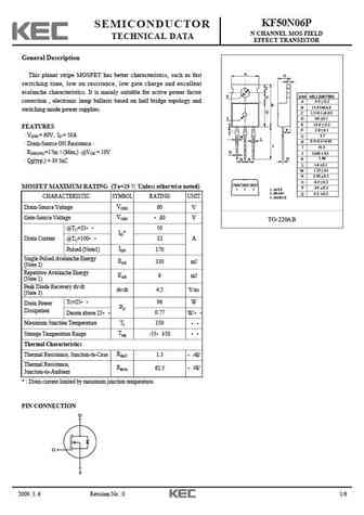
KF50N06P SEMICONDUCTOR N CHANNEL MOS FIELD TECHNICAL DATA EFFECT TRANSISTOR General Description A This planar stripe MOSFET has better characteristics, such as fast O C switching time, low on resistance, low gate charge and excellent F avalanche characteristics. It is mainly suitable for active power factor E DIM MILLIMETERS G _ correction , electronic lamp ballasts based on hal... See More ⇒
cep50n06 ceb50n06.pdf
CEP50N06/CEB50N06 N-Channel Enhancement Mode Field Effect Transistor FEATURES 60V, 50A ,RDS(ON) = 17m (typ) @VGS = 10V. Super high dense cell design for extremely low RDS(ON). High power and current handing capability. D Lead free product is acquired. TO-220 & TO-263 package. G CEB SERIES CEP SERIES S TO-263(DD-PAK) TO-220 ABSOLUTE MAXIMUM RATINGS Tc = 25 C unless otherwise no... See More ⇒
am50n06-15d.pdf
Analog Power AM50N06-15D N-Channel 60-V (D-S) MOSFET PRODUCT SUMMARY Key Features rDS(on) (m ) VDS (V) ID(A) Low r trench technology DS(on) 13 @ VGS = 10V 51 Low thermal impedance 60 18 @ VGS = 4.5V 44 Fast switching speed Typical Applications White LED boost converters Automotive Systems Industrial DC/DC Conversion Circuits ABSOLUTE MAXIMUM... See More ⇒
am50n06-20d.pdf
Analog Power AM50N06-20D N-Channel 60-V (D-S) MOSFET These miniature surface mount MOSFETs utilize a PRODUCT SUMMARY high cell density trench process to provide low VDS (V) rDS(on) m( ) ID (A) rDS(on) and to ensure minimal power loss and heat dissipation. Typical applications are DC-DC 20 @ VGS = 10V 41 converters and power management in portable and 60 29 @ VGS = 4.5V 34 batte... See More ⇒
jcs50n06vh jcs50n06rh jcs50n06ch jcs50n06fh.pdf
N R N-CHANNEL MOSFET JCS50N06H Package MAIN CHARACTERISTICS ID 50 A VDSS 60 V Rdson-max 23 m @Vgs=10V Qg-typ 34 nC APPLICATIONS High frequency switch UPS mode power supplies UPS FEATURES Low gate charge ... See More ⇒
jt050n065wed.pdf
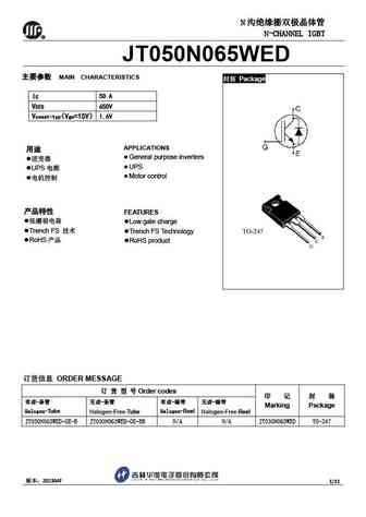
N N-CHANNEL IGBT R JT050N065WED MAIN CHARACTERISTICS Package IC 50 A VCES 650V Vcesat-typ 1.6V Vge=15V APPLICATIONS General purpose inverters UPS UPS Motor control FEATURES Low gate charge Trench FS... See More ⇒
mtn50n06e3.pdf
Spec. No. C445E3 Issued Date 2009.05.12 CYStech Electronics Corp. Revised Date 2013.02.26 Page No. 1/8 N-Channel Enhancement Mode Power MOSFET BVDSS 60V RDSON(MAX) 22 m MTN50N06E3 ID 50A Description The MTN50N06E3 is a N-channel enhancement-mode MOSFET, providing the designer with the best combination of fast switching, ruggedized device design, low on-resistance ... See More ⇒
brcs50n06bd.pdf
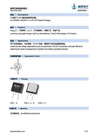
BRCS50N06BD Rev.A Sep.-2022 DATA SHEET / Descriptions N TO-263 N-CHANNEL MOSFET in a TO-263 Plastic Package. / Features R C DS(on) rss Low R ,low gate charge, low C , fast switching, Trench Technologies, HF Product. DS(on) rss / Applications ... See More ⇒
brcs50n06ra.pdf
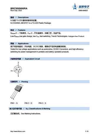
BRCS50N06RA Rev.A Sep.-2020 DATA SHEET / Descriptions N TO-220 N-CHANNEL MOSFET in a TO-220 Plastic Package. / Features R C DS(on) rss Low RDS(on),low gate charge, low Crss, fast switching, Trench Technologies. Halogen-free Product. / Applications ... See More ⇒
brcs50n06dp.pdf
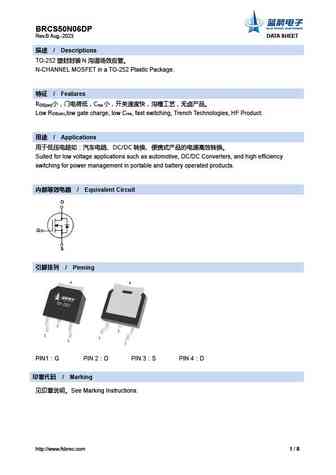
BRCS50N06DP Rev.B Aug.-2023 DATA SHEET / Descriptions TO-252 N N-CHANNEL MOSFET in a TO-252 Plastic Package. / Features R C DS(on) rss Low R ,low gate charge, low C , fast switching, Trench Technologies, HF Product. DS(on) rss / Applications ... See More ⇒
brd50n06.pdf
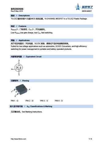
BRD50N06 Rev.D May.-2016 DATA SHEET / Descriptions TO-252 N MOS N-CHANNEL MOSFET in a TO-252 Plastic Package. / Features R C DS(on) rss Low RDS(on),low gate charge, low Crss, fast switching. / Applications DC/DC ... See More ⇒
brb50n06.pdf
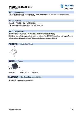
BRB50N06(BRCS50N06B) Rev.C Feb.-2015 DATA SHEET / Descriptions TO-263 N MOS N-CHANNEL MOSFET in a TO-252 Plastic Package. / Features R C DS(on) rss Low RDS(on),low gate charge, low Crss, fast switching. / Applications DC/DC ... See More ⇒
br50n06.pdf
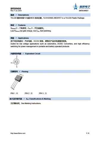
BR50N06 Rev. F Jul.-2018 DATA SHEET / Descriptions TO-220 N MOS N-CHANNEL MOSFET in a TO-220 Plastic Package. / Features R C DS(on) rss Low RDS(on),low gate charge, low Crss, fast switching. / Applications DC/DC ... See More ⇒
bri50n06.pdf
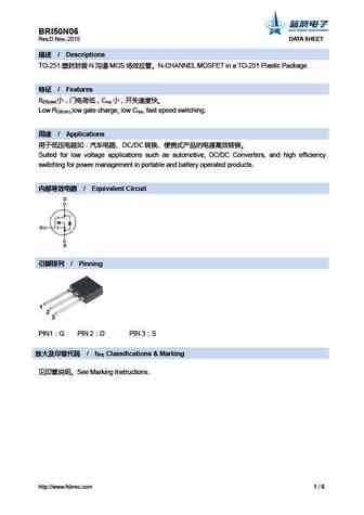
BRI50N06 Rev.D Nov.-2015 DATA SHEET / Descriptions TO-251 N MOS N-CHANNEL MOSFET in a TO-251 Plastic Package. / Features R C DS(on) rss Low RDS(on),low gate charge, low Crss, fast speed switching. / Applications DC/DC ... See More ⇒
50n06a 50n06af 50n06f 50n06g.pdf
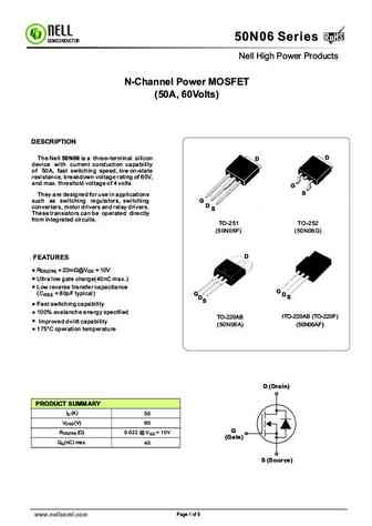
RoHS 50N06 Series RoHS SEMICONDUCTOR Nell High Power Products N-Channel Power MOSFET (50A, 60Volts) DESCRIPTION D The Nell 50N06 is a three-terminal silicon D device with current conduction capability of 50A, fast switching speed, low on-state resistance, breakdown voltage rating of 60V, and max. threshold voltage of 4 volts. G S They are designed for use in applications ... See More ⇒
hfp50n06.pdf
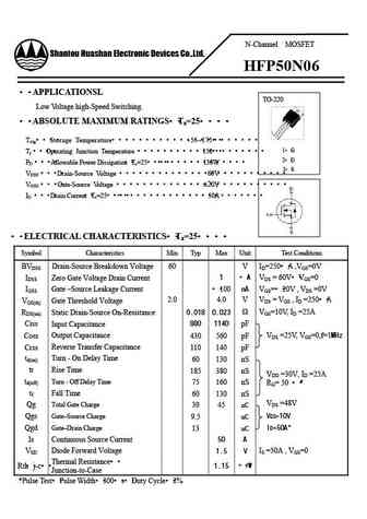
N-Channel MOSFET Shantou Huashan Electronic Devices Co.,Ltd. HFP50N06 APPLICATIONSL TO-220 Low Voltage high-Speed Switching. ABSOLUTE MAXIMUM RATINGS Ta=25 Tstg Storage Temperature -55 175 1 G Tj Operating Junction Temperature 150 2 D PD Allowable Power Dissipation ... See More ⇒
hfp50n06v.pdf
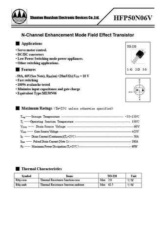
Shantou Huashan Electronic Devices Co.,Ltd. HFP50N06V N-Channel Enhancement Mode Field Effect Transistor Applications TO-220 Servo motor control. DC/DC converters Low Power Switching mode power appliances. Other switching applications. 1- G 2-D 3-S Features 50A, 60V(See Note), RDS(on) ... See More ⇒
irf50n06.pdf
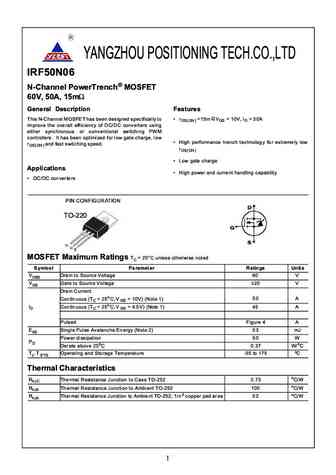
3 0 lmnopqrsurvwxwrnwnoxyzq zr x 45367879 8 3 97 67 6!" # $ % &0'& 3 'R % ()*+-./)0112345678()0+9221 2+*;12 +*=033?@A QCE6O5-PS2TB"NUV6S2WUNLESXWY *B>*=*21=?A>E/FE/=A1D2C@2C+G+*1; 2*@)2C +?1=)CA1AG+ AC =A1D21@*A103+H*@=)*1; IJ4 =A1@CA332C+KL@)0+9221AAC3AH;0@2=)0C;2N3AH QZ*;)ACB01=2@C21=)@2=)1A3A;?>AC2[@C2B23?3AH CE6O5-P01 >0+@+H*@=)*1;+... See More ⇒
cm50n06.pdf
R CM50N06 www.jdsemi.cn ShenZhen Jingdao Electronic Co.,Ltd. POWER MOSFET 60V N-Channel Trench-MOS RoHS 1 2 3 TO-220 4 ... See More ⇒
ftk50n06d.pdf
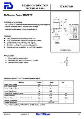
SEMICONDUCTOR FTK50N06D TECHNICAL DATA N-Channel Power MOSFET A I C J GENERAL DESCRIPTION The FTK50N06D uses advanced trench technology and design to DIM MILLIMETERS A 6 50 0 2 provide excellent RDS(ON) with low gate charge. B 5 60 0 2 C 5 20 0 2 It can be used in awide variety of applications. D 1 50 0 2 E 2 70 0 2 F 2 30 0 1 H H 1 00 MAX I 2 30 0... See More ⇒
ftk50n06 ftk50n06p f.pdf
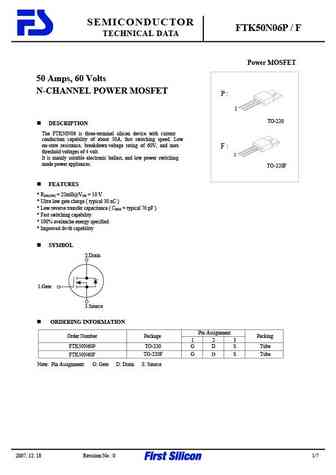
SEMICONDUCTOR FTK50N06P / F TECHNICAL DATA Power MOSFET 50 Amps, 60 Volts N-CHANNEL POWER MOSFET P 1 TO-220 DESCRIPTION The FTK50N06 is three-terminal silicon device with current conduction capability of about 50A, fast switching speed. Low on-state resistance, breakdown voltage rating of 60V, and max F threshold voltages of 4 volt. 1 It is mainly suitable electronic ... See More ⇒
ftk50n06dd.pdf
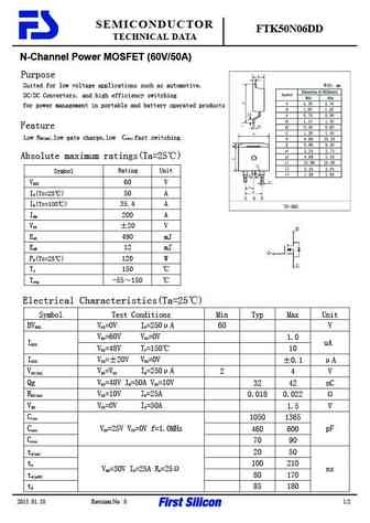
SEMICONDUCTOR FTK50N06DD TECHNICAL DATA N-Channel Power MOSFET (60V/50A) Purpose Suited for low voltage applications such as automotive, DC/DC Converters, and high efficiency switching for power management in portable and battery operated products Feature Low RDS(on),low gate charge,low Crss,fast switching. Absolute maximum ratings(Ta=25 ) Rating Symbol Unit V 60 V DSS ... See More ⇒
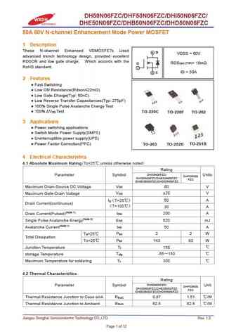
dh50n06fzc dhf50n06fzc dhi50n06fzc dhe50n06fzc dhb50n06fzc dhd50n06fzc.pdf
... See More ⇒
svd50n06t svd50n06d svd50n06m svd50n06mj.pdf
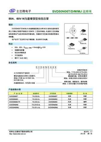
SVD50N06T/D/M/MJ 50A 60V N 2 SVD50N06T/D/M/MJ N MOS VDMOS 1 1 3 TO-252-2L 3 ... See More ⇒
ms50n06.pdf
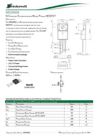
MS50N06 N-Channel Enhancement Mode Power MOSFET Description The MS50N60 is a N-channel enhancement-mode MOSFET , providing the designer with the best combination of fast switching, ruggedized device design, low on-resistance and cost effectiveness. The TO-220F package is universally preferred for all commercial-industrial applications Features Low On Resistance Sim... See More ⇒
sfp50n06r.pdf
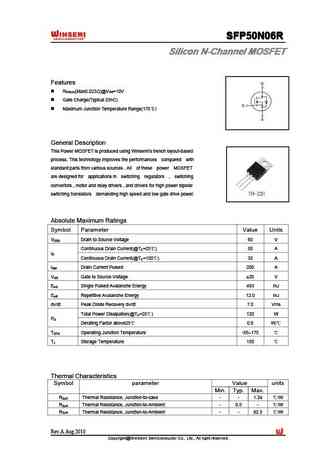
SFP50N06R SFP50N06R SFP50N06R SFP50N06R Silicon N-Channel MOSFET Silicon N-Channel MOSFET Silicon N-Channel MOSFET Silicon N-Channel MOSFET Features R (Max0.023 )@V =10V DS(on) GS Gate Charge(Typical 25nC) Maximum Junction Temperature Range(175 ) General Description This Power MOSFET is produced using Winsemi s trench layout-based process. This technology improv... See More ⇒
wfp50n06c.pdf
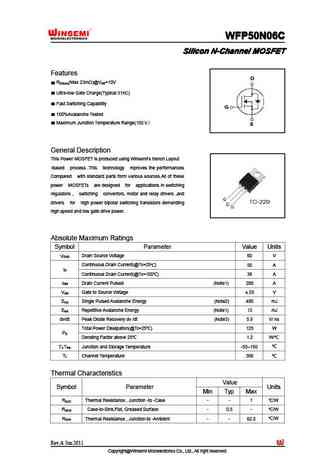
WFP50N06C WFP50N06C WFP50N06C WFP50N06C Silicon N-Channel MOSFET Silicon N-Channel MOSFET Silicon N-Channel MOSFET Silicon N-Channel MOSFET Features R (Max 23m )@V =10V DS(on) GS Ultra-low Gate Charge(Typical 31nC) Fast Switching Capability 100%Avalanche Tested Maximum Junction Temperature Range(150 ) General Description This Power MOSFET is produced usin... See More ⇒
wfp50n06.pdf
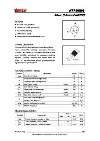
WFP50N06 WFP50N06 WFP50N06 WFP50N06 Silicon N-Channel MOSFET Silicon N-Channel MOSFET Silicon N-Channel MOSFET Silicon N-Channel MOSFET Features R (Max 22m )@V =10V DS(on) GS Ultra-low Gate Charge(Typical 31nC) Fast Switching Capability 100%Avalanche Tested Maximum Junction Temperature Range(150 ) General Description This Power MOSFET is produced using Wi... See More ⇒
sfp50n06.pdf
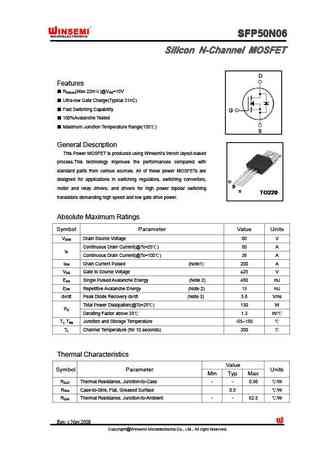
SFP50N06 SFP50N06 SFP50N06 SFP50N06 Silicon N-Channel MOSFET Silicon N-Channel MOSFET Silicon N-Channel MOSFET Silicon N-Channel MOSFET Features R (Max 22m )@V =10V DS(on) GS Ultra-low Gate Charge(Typical 31nC) Fast Switching Capability 100%Avalanche Tested Maximum Junction Temperature Range(150 ) General Description This Power MOSFET is produced using Win... See More ⇒
chm50n06pagp.pdf
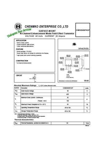
CHENMKO ENTERPRISE CO.,LTD CHM50N06PAGP SURFACE MOUNT N-Channel Enhancement Mode Field Effect Transistor VOLTAGE 60 Volts CURRENT 36 Ampere APPLICATION * Servo motor control. * Power MOSFET gate drivers. * Other switching applications. D-PAK(TO-252) FEATURE * Small package. (TO-252) * Super high dense cell design for extremely low RDS(ON). .094 (2.40) .280 (7.10) * High power... See More ⇒
chm50n06ngp.pdf
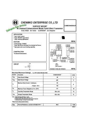
CHENMKO ENTERPRISE CO.,LTD CHM50N06NGP SURFACE MOUNT N-Channel Enhancement Mode Field Effect Transistor VOLTAGE 60 Volts CURRENT 50 Ampere APPLICATION * Servo motor control. * Power MOSFET gate drivers. * Other switching applications. D2PAK FEATURE * Small package. (D2PAK) 0.420(10.67) 0.190(4.83) * Super high dense cell design for extremely low RDS(ON). 0.380(9.69) 0.160(4.... See More ⇒
fhp50n06 fhu50n06d fhd50n06d.pdf
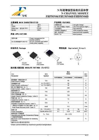
N N-CHANNEL MOSFET FHP50N06/FHU50N06D/FHD50N06D MAIN CHARACTERISTICS FEATURES ID 50 A Low gate charge VDSS 60 V Crss ( 130pF) Low Crss (typical 130pF ) Rdson-typ @Vgs=10V 8.5m Fast switching Qg-typ 40nC 100% 100% avalanche tested dv/dt... See More ⇒
fha150n06c.pdf
N N-CHANNEL MOSFET FHA150N06C MAIN CHARACTERISTICS FEATURES ID 150 A Low gate charge VDSS 55 V Crss ( 850pF) Low Crss (typical 850pF ) Rdson-typ @Vgs=10V 7.2 m Fast switching Qg-typ 118nC 100% 100% avalanche tested dv/dt Improved ... See More ⇒
kia50n06b.pdf
50A 60V 50N06B N-CHANNELMOSFET KIA KIA KIA SEMICONDUCTORS SEMICONDUCTORS SEMICONDUCTORS 1. Features R =10.5m @ V =10V DS(on) GS Lead free and green device available Low Rds-on to minimize conductive loss High avalanche current 2. Applications Power supply UPS Battery management system 3.Symbol Pin Function 1 Gate 2 Drain 3 Source 4 Drain 1of 6 Rev 1.1JAN2014 ... See More ⇒
me50n06a me50n06a-g.pdf
ME50N06A/ME50N06A-G N- Channel 60V (D-S) MOSFET GENERAL DESCRIPTION FEATURES The ME50N06A is the N-Channel logic enhancement mode power RDS(ON) 22m @VGS=10V field effect transistors are produced using high cell density DMOS Super high density cell design for extremely low RDS(ON) trench technology. This high density process is especially tailored to Exceptional on-resi... See More ⇒
me50n06t me50n06t-g.pdf
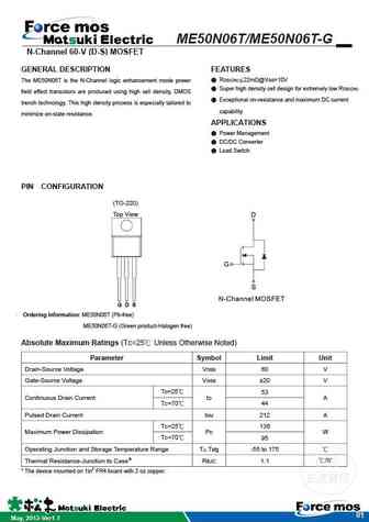
ME50N06T/ME50N06T-G N-Channel 60-V (D-S) MOSFET GENERAL DESCRIPTION FEATURES RDS(ON) 22m @VGS=10V The ME50N06T is the N-Channel logic enhancement mode power Super high density cell design for extremely low RDS(ON) field effect transistors are produced using high cell density, DMOS Exceptional on-resistance and maximum DC current trench technology. This high densit... See More ⇒
sw50n06.pdf
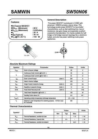
SAMWIN SW50N06 General Description Features This power MOSFET is produced in CHMC with advanced VDMOS process, planar stripe. This N-Channel MOSFET technology enable power MOSFET to have better BVDSS (Minimum) 60V characteristics, such as fast switching time, low on RDS(ON) (Maximum) 0.023ohm resistance, low gate charge and especially excellent ID 50 A avalanche character... See More ⇒
sre50n065fsud6.pdf
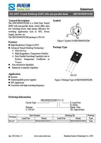
Datasheet 50A 650V Trench Fieldstop IGBT with anti-parallel diode SRE50N065FSUD6 General Description Symbol The SRE50N065FSUD6 is a Field Stop Trench IGBT with anti-parallel diode, which offers ultra low switching losses, high energy efficiency for switching applications such as PFC, Power Supply, Inverter, etc. The SRE50N065FSUD6 package is TO-247. Figure 1 Symbol of SRE50N... See More ⇒
sre50n065fsu.pdf
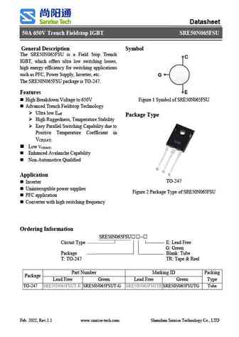
Datasheet 50A 650V Trench Fieldstop IGBT SRE50N065FSU General Description Symbol The SRE50N065FSU is a Field Stop Trench C IGBT, which offers ultra low switching losses, high energy efficiency for switching applications such as PFC, Power Supply, Inverter, etc. G The SRE50N065FSU package is TO-247. E Features High Breakdown Voltage to 650V Figure 1 Symbol of SRE50N065... See More ⇒
hfs50n06.pdf
July 2005 BVDSS = 60 V RDS(on) = 18 m HFS50N06 ID = 50 A 60V N-Channel MOSFET TO-220F FEATURES 1 Originative New Design 2 3 Superior Avalanche Rugged Technology 1.Gate 2. Drain 3. Source Robust Gate Oxide Technology Very Low Intrinsic Capacitances Excellent Switching Characteristics Unrivalled Gate Charge 40 nC (Typ.) Extended Safe Operating Area Lower RDS(ON) ... See More ⇒
hfp50n06a hfs50n06a.pdf
Oct 2016 HFP50N06A / HFS50N06A 60V N-Channel MOSFET Features Key Parameters Parameter Value Unit Superior Avalanche Rugged Technology BVDSS 60 V Robust Gate Oxide Technology Very Low Intrinsic Capacitances ID 50 A Excellent Switching Characteristics RDS(on), Typ 18 100% Avalanche Tested Qg, Typ 27 nC RoHS Compliant HFP50N06A HFS50N06A Symbol TO-220 TO-220F S S... See More ⇒
hfi50n06a hfw50n06a.pdf
Oct 2016 HFI50N06A / HFW50N06A 60V N-Channel MOSFET Features Key Parameters Parameter Value Unit Superior Avalanche Rugged Technology BVDSS 60 V Robust Gate Oxide Technology Very Low Intrinsic Capacitances ID 50 A Excellent Switching Characteristics RDS(on), Typ 18 100% Avalanche Tested Qg, Typ 27 nC RoHS Compliant HFI50N06A HFW50N06A Symbol TO-262 TO-263 D S ... See More ⇒
hrd50n06k hru50n06k.pdf
Sep 2015 BVDSS = 60 V RDS(on) typ HRD50N06K / HRU50N06K ID = 40 A 60V N-Channel Trench MOSFET D-PAK I-PAK FEATURES 2 1 Originative New Design 1 3 2 3 Superior Avalanche Rugged Technology HRD50N06K HRU50N06K Excellent Switching Characteristics 1.Gate 2. Drain 3. Source Unrivalled Gate Charge 40 nC (Typ.) Extended Safe Operating Area Lower RDS(ON) 11.... See More ⇒
hfi50n06 hfw50n06.pdf
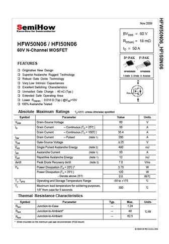
Nov 2009 BVDSS = 60 V RDS(on) = 18 m HFW50N06 / HFI50N06 ID = 50 A 60V N-Channel MOSFET D2-PAK I2-PAK FEATURES Originative New Design HFW50N06 HFI50N06 Superior Avalanche Rugged Technology 1.Gate 2. Drain 3. Source Robust Gate Oxide Technology Very Low Intrinsic Capacitances Excellent Switching Characteristics Unrivalled Gate Charge 40 nC (Typ.) Extended Safe Operati... See More ⇒
sii150n06.pdf
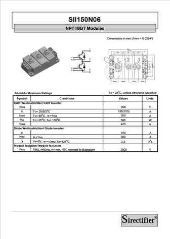
SII150N06 NPT IGBT Modules Dimensions in mm (1mm = 0.0394") TC = 25oC, unless otherwise specified Absolute Maximum Ratings Symbol Conditions Values Units IGBT Wechselrichter/ IGBT Inverter VCES 600 V IC 180(150) TC= 25(60)oC A ICRM 300 TC= 60oC, tP =1ms A Ptot TC= 25oC, Tvj= 150oC 595 W _ VGES +20 V Diode Wechselrichter/ Diode Inverter IF 150 A IFRM 300 tP =1ms A 2 VR... See More ⇒
sii50n06.pdf
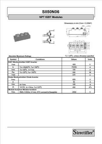
SII50N06 NPT IGBT Modules Dimensions in mm (1mm = 0.0394") TC = 25oC, unless otherwise specified Absolute Maximum Ratings Symbol Conditions Values Units IGBT Wechselrichter/ IGBT Inverter VCES 600 V IC 75(50) TC= 25(80)oC, Tvj= 150oC A ICRM 100 TC= 80oC, tP =1ms A Ptot TC= 25oC, Tvj= 150oC 280 W _ VGES +20 V Diode Wechselrichter/ Diode Inverter VRRM 600 V IF 50 A IFRM 10... See More ⇒
sg50n06dt.pdf
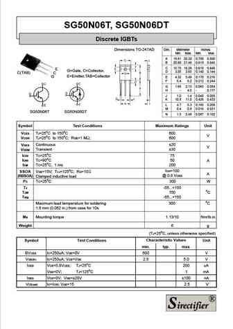
SG50N06T, SG50N06DT Discrete IGBTs Dimensions TO-247AD Dim. Millimeter Inches Min. Max. Min. Max. A 19.81 20.32 0.780 0.800 B 20.80 21.46 0.819 0.845 C 15.75 16.26 0.610 0.640 E G=Gate, C=Collector, D 3.55 3.65 0.140 0.144 C(TAB) C E=Emitter,TAB=Collector G E 4.32 5.49 0.170 0.216 F 5.4 6.2 0.212 0.244 G 1.65 2.13 0.065 0.084 H - 4.5 - 0.177 J 1.0 1.4 0.040 0.055 K 10.8 11.0 ... See More ⇒
sg50n06t.pdf

SG50N06T, SG50N06DT Discrete IGBTs Dimensions TO-247AD Dim. Millimeter Inches Min. Max. Min. Max. A 19.81 20.32 0.780 0.800 B 20.80 21.46 0.819 0.845 C 15.75 16.26 0.610 0.640 E G=Gate, C=Collector, D 3.55 3.65 0.140 0.144 C(TAB) C E=Emitter,TAB=Collector G E 4.32 5.49 0.170 0.216 F 5.4 6.2 0.212 0.244 G 1.65 2.13 0.065 0.084 H - 4.5 - 0.177 J 1.0 1.4 0.040 0.055 K 10.8 11.0 ... See More ⇒
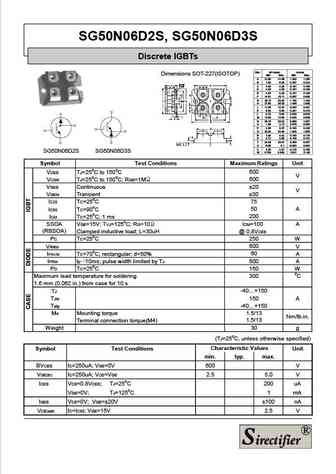
sg50n06d2s.pdf

SG50N06D2S, SG50N06D3S Discrete IGBTs Dim. Millimeter Inches Dimensions SOT-227(ISOTOP) Min. Max. Min. Max. A 31.50 31.88 1.240 1.255 B 7.80 8.20 0.307 0.323 C 4.09 4.29 0.161 0.169 D 4.09 4.29 0.161 0.169 E 4.09 4.29 0.161 0.169 F 14.91 15.11 0.587 0.595 G 30.12 30.30 1.186 1.193 H 37.80 38.20 1.489 1.505 J 11.68 12.22 0.460 0.481 K 8.92 9.60 0.351 0.378 L 0.76 0.84 0.030 0.033 ... See More ⇒
sg50n06s.pdf

SG50N06S, SG50N06DS Discrete IGBTs C Dim. Millimeter Inches E Dimensions SOT-227(ISOTOP) Min. Max. Min. Max. A 31.50 31.88 1.240 1.255 B 7.80 8.20 0.307 0.323 C 4.09 4.29 0.161 0.169 D 4.09 4.29 0.161 0.169 E 4.09 4.29 0.161 0.169 G=Gate, C=Collector, F 14.91 15.11 0.587 0.595 G 30.12 30.30 1.186 1.193 E=Emitter H 37.80 38.20 1.489 1.505 J 11.68 12.22 0.460 0.481 K 8.92 9.60 0... See More ⇒
sg50n06d3s.pdf
SG50N06D2S, SG50N06D3S Discrete IGBTs Dim. Millimeter Inches Dimensions SOT-227(ISOTOP) Min. Max. Min. Max. A 31.50 31.88 1.240 1.255 B 7.80 8.20 0.307 0.323 C 4.09 4.29 0.161 0.169 D 4.09 4.29 0.161 0.169 E 4.09 4.29 0.161 0.169 F 14.91 15.11 0.587 0.595 G 30.12 30.30 1.186 1.193 H 37.80 38.20 1.489 1.505 J 11.68 12.22 0.460 0.481 K 8.92 9.60 0.351 0.378 L 0.76 0.84 0.030 0.033 ... See More ⇒
sg50n06ds.pdf
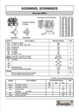
SG50N06S, SG50N06DS Discrete IGBTs C Dim. Millimeter Inches E Dimensions SOT-227(ISOTOP) Min. Max. Min. Max. A 31.50 31.88 1.240 1.255 B 7.80 8.20 0.307 0.323 C 4.09 4.29 0.161 0.169 D 4.09 4.29 0.161 0.169 E 4.09 4.29 0.161 0.169 G=Gate, C=Collector, F 14.91 15.11 0.587 0.595 G 30.12 30.30 1.186 1.193 E=Emitter H 37.80 38.20 1.489 1.505 J 11.68 12.22 0.460 0.481 K 8.92 9.60 0... See More ⇒
sl50n06d sl50n06i.pdf
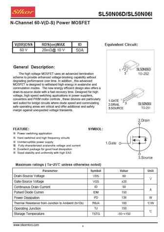
SL50N06D/SL50N06I N-Channel 60-V(D-S) Power MOSFET V(BR)DSS RDS(on)MAX ID Equivalent Circuit 60 V 20m @ 10 V 50A General Description 2 SL50N06D The high voltage MOSFET uses an advanced termination 3 scheme to provide enhanced voltage-blocking capability without degrading performance over time. In addition , this advanced MOSFET is designed to withstand high energy in avalanche ... See More ⇒
dfp50n06.pdf

DFP50N06 Pb DFP50N06 Pb Free Plating Product 50A,60V Heatsink Planar N-Channel Power MOSFET Features 2. Drain 50A, 60V, RDS(on) = 0.022 @VGS = 10 V BVDSS = 60V Low gate charge ( typical 31 nC) Low Crss ( typical 65 pF) RDS(ON) = 0.022 ohm Fast switching 1. Gate 100% avalanche tested ID = 50A ... See More ⇒
wmk50n06ts.pdf
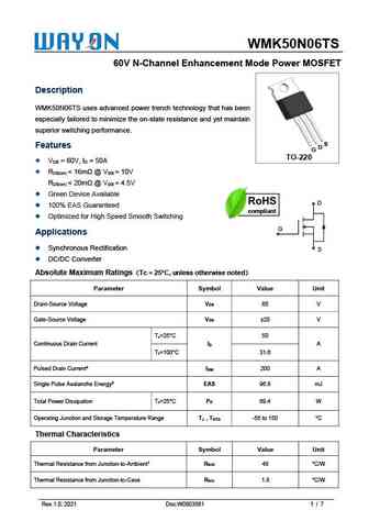
WMK50N06TS 60V N-Channel Enhancement Mode Power MOSFET Description WMK50N06TS uses advanced power trench technology that has been especially tailored to minimize the on-state resistance and yet maintain superior switching performance. S Features D G TO-220 V = 60V, I = 50A DS D R ... See More ⇒
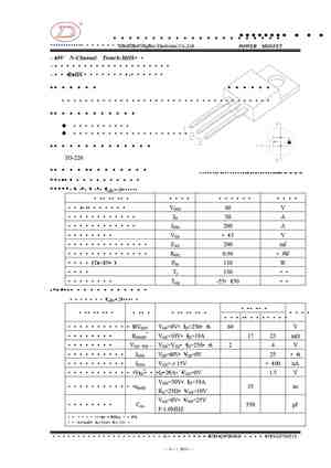
ad50n06s.pdf
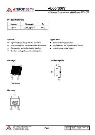
AD50N06S N-Channel Enhancement Mode Power MOSFET Product Summary V(BR)DSS RDS(on)MAX ID 60V 20m @10V 50A Feature Application High density cell design for ultra low Rdson Power switching application Fully characterized avalanche voltage and current Hard switched and high frequency circuits Good stability and uniformity with high EAS Uninterruptible power supply Excellent p... See More ⇒
cs50n06f cs50n06p cs50n06u cs50n06d.pdf
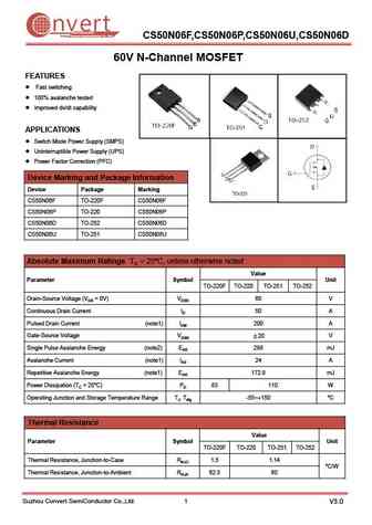
nvert Suzhou Convert Semiconductor Co ., Ltd. CS50N06F,CS50N06P,CS50N06U,CS50N06D 60V N-Channel MOSFET FEATURES Fast switching 100% avalanche tested Improved dv/dt capability APPLICATIONS Switch Mode Power Supply (SMPS) Uninterruptible Power Supply (UPS) Power Factor Correction (PFC) Device Marking and Package Information Device Package Marking CS50N06F TO-... See More ⇒
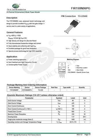
fir150n06pg.pdf
FIR150N06PG N-Channel Enhancement Mode Power Mosfet PIN Connection TO-220AB Description The FIR150N06G uses advanced trench technology and design to provide excellent RDS(ON) with low gate charge. It can be used in a wide variety of applications. General Features VDS =60V,ID =150A RDS(ON) ... See More ⇒
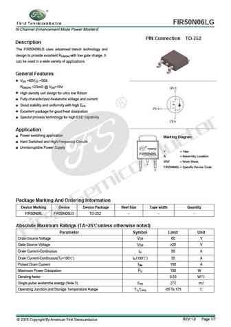
fir50n06lg.pdf
FIR50N06LG N-Channel Enhancement Mode Power Mosfet-E PIN Connection TO-252 Description The FIR50N06LG uses advanced trench technology and design to provide excellent RDS(ON) with low gate charge. It can be used in a wide variety of applications. General Features VDS =60V,ID =50A RDS(ON) ... See More ⇒
hd50n06d hu50n06d.pdf
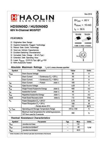
Nov 2019 BVDSS = 60 V RDS(on) = 15 m HD50N06D / HU50N06D ID = 50 A 60V N-Channel MOSFET TO-252 TO-251 FEATURES Originative New Design HD50N06D HU50N06D Superior Avalanche Rugged Technology 1.Gate 2. Drain 3. Source Robust Gate Oxide Technology Very Low Intrinsic Capacitances Excellent Switching Characteristics Unrivalled Gate Charge 40 nC (Typ.) ... See More ⇒
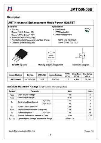
jmti50n06b.pdf
JMTI50N06B Description JMT N-channel Enhancement Mode Power MOSFET Features Application 60V,50A Load Switch R ... See More ⇒
jmtk50n06b.pdf
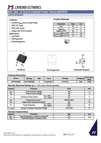
60V, 50A, 13.7m N-channel Power Trench MOSFET JMTK50N06B Product Summary Features Excellent RDS(ON) and Low Gate Charge Parameters Value Unit 100% UIS Tested VDSS 60 V 100% Vds Tested VGS(th)_Typ 1.6 V Halogen-free; RoHS-compliant ID(@VGS=10V) 50 A RDS(ON)_Typ(@VGS=10V 12.2 mW Applications RDS(ON)_Typ(@VGS=4.5V 13.7 mW Load Switch PWM Application ... See More ⇒
ptd50n06.pdf
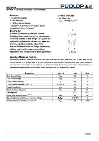
PTD50N06 60V/50A N-Channel Advanced Power MOSFET Features General Features Low On-Resistance VDS =60V,ID =50A Fast Switching RDS(ON) ... See More ⇒
sk50n06a.pdf
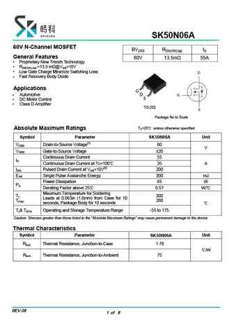
SK50N06A 60V N-Channel MOSFET BVDSS RDS(ON),typ. ID General Features 60V 13.5m 55A Proprietary New Trench Technology RDS(ON),typ.=13.5 m @VGS=10V Low Gate Charge Minimize Switching Loss Fast Recovery Body Diode Applications G Automotive D S DC Motor Control Class D Amplifier TO-252 Package No to Scale T =25 unless otherwise sp... See More ⇒
tx50n06.pdf
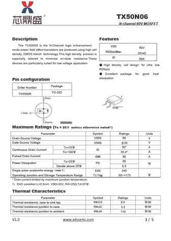
TX50N06 N channel 60V MOSFET Description Features The TX50N06 is the N-Channel logic enhancement VDS 60V mode power field effect transistors are produced using high cell RDS(on)Max. 20m density, DMOS trench technology.This high density process is ID especially tailored to minimize on-state resistance.These 50A devices are particularly suited for low voltage application. High... See More ⇒
vbzm50n06.pdf
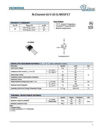
VBZM50N06 www.VBsemi.com N-Channel 60-V (D-S) MOSFET FEATURES PRODUCT SUMMARY 175 C Junction Temperature VDS (V) RDS(on) ( ) ID (A)a TrenchFET Power MOSFET 0.011 at VGS = 10 V 60 Material categorization 60 0.013 at VGS = 4.5 V 50 D TO-220AB G S D S G N-Channel MOSFET ABSOLUTE MAXIMUM RATINGS (TC = 25 C, unless otherwise noted) Parameter Symbol Lim... See More ⇒
cmd50n06b.pdf

CMD50N06B www.VBsemi.tw N-Channel 60 V (D-S) MOSFET FEATURES PRODUCT SUMMARY 175 C Junction Temperature VDS (V) RDS(on) ( ) ID (A)a TrenchFET Power MOSFET 0.012 at VGS = 10 V 50 Material categorization 60 0.013 at VGS = 4.5 V 45 D TO-252 G S G D S N-Channel MOSFET ABSOLUTE MAXIMUM RATINGS (TC = 25 C, unless otherwise noted) Parameter Symbol Limit ... See More ⇒
hs50n06da.pdf

HS50N06DA www.VBsemi.tw N-Channel 60 V (D-S) MOSFET FEATURES PRODUCT SUMMARY 175 C Junction Temperature VDS (V) RDS(on) ( ) ID (A)a TrenchFET Power MOSFET 0.012 at VGS = 10 V 50 Material categorization 60 0.013 at VGS = 4.5 V 45 D TO-252 G S G D S N-Channel MOSFET ABSOLUTE MAXIMUM RATINGS (TC = 25 C, unless otherwise noted) Parameter Symbol Limit ... See More ⇒
vbzfb50n06.pdf
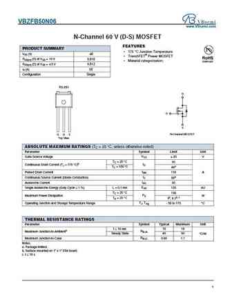
VBZFB50N06 www.VBsemi.com N-Channel 60 V (D-S) MOSFET FEATURES PRODUCT SUMMARY 175 C Junction Temperature VDS (V) 60 TrenchFET Power MOSFET RDS(on) ( ) at VGS = 10 V 0.010 Material categorization RDS(on) ( ) at VGS = 4.5 V 0.012 ID (A) 50 Configuration Single TO-251 D G S N-Channel MOSFET G D S Top View ABSOLUTE MAXIMUM RATINGS (TC = 25 C, unless other... See More ⇒
ceu50n06.pdf

CEU50N06 www.VBsemi.tw N-Channel 60 V (D-S) MOSFET FEATURES PRODUCT SUMMARY 175 C Junction Temperature VDS (V) RDS(on) ( ) ID (A)a TrenchFET Power MOSFET 0.012 at VGS = 10 V 50 Material categorization 60 0.013 at VGS = 4.5 V 45 D TO-252 G S G D S N-Channel MOSFET ABSOLUTE MAXIMUM RATINGS (TC = 25 C, unless otherwise noted) Parameter Symbol Limit U... See More ⇒
fqd50n06.pdf
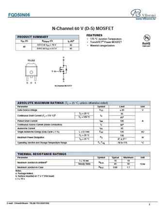
FQD50N06 www.VBsemi.tw N-Channel 60 V (D-S) MOSFET FEATURES PRODUCT SUMMARY 175 C Junction Temperature VDS (V) RDS(on) ( ) ID (A)a TrenchFET Power MOSFET 0.012 at VGS = 10 V 50 Material categorization 60 0.013 at VGS = 4.5 V 45 D TO-252 G S G D S N-Channel MOSFET ABSOLUTE MAXIMUM RATINGS (TC = 25 C, unless otherwise noted) Parameter Symbol Limit U... See More ⇒
vbze50n06.pdf
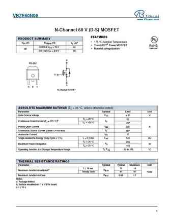
VBZE50N06 www.VBsemi.com N-Channel 60 V (D-S) MOSFET FEATURES PRODUCT SUMMARY 175 C Junction Temperature VDS (V) RDS(on) ( ) ID (A)a TrenchFET Power MOSFET 0.009 at VGS = 10 V 60 Material categorization 60 0.011at VGS = 4.5 V 50 D TO-252 G S G D S N-Channel MOSFET ABSOLUTE MAXIMUM RATINGS (TC = 25 C, unless otherwise noted) Parameter Symbol Limit ... See More ⇒
ipd50n06s2-14.pdf

IPD50N06S2-14 www.VBsemi.tw N-Channel 60 V (D-S) MOSFET FEATURES PRODUCT SUMMARY 175 C Junction Temperature VDS (V) RDS(on) ( ) ID (A)a TrenchFET Power MOSFET 0.012 at VGS = 10 V 50 Material categorization 60 0.013 at VGS = 4.5 V 45 D TO-252 G S G D S N-Channel MOSFET ABSOLUTE MAXIMUM RATINGS (TC = 25 C, unless otherwise noted) Parameter Symbol Li... See More ⇒
fqb50n06.pdf
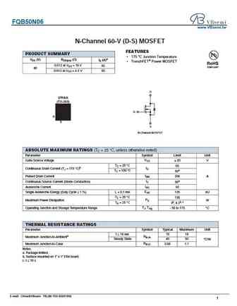
FQB50N06 www.VBsemi.tw N-Channel 60-V (D-S) MOSFET FEATURES PRODUCT SUMMARY 175 C Junction Temperature VDS (V) RDS(on) ( ) ID (A)a TrenchFET Power MOSFET 0.012 at VGS = 10 V 60 60 0.013 at VGS = 4.5 V 50 D D2PAK (TO-263) G G D S S N-Channel MOSFET ABSOLUTE MAXIMUM RATINGS (TC = 25 C, unless otherwise noted) Parameter Symbol Limit Unit VGS Gate-Source... See More ⇒
sud50n06-09l.pdf
SUD50N06-09L www.VBsemi.tw N-Channel 60 V (D-S) MOSFET FEATURES PRODUCT SUMMARY 175 C Junction Temperature VDS (V) RDS(on) ( ) ID (A)a TrenchFET Power MOSFET 0.012 at VGS = 10 V 50 Material categorization 60 0.013 at VGS = 4.5 V 45 D TO-252 G S G D S N-Channel MOSFET ABSOLUTE MAXIMUM RATINGS (TC = 25 C, unless otherwise noted) Parameter Symbol Lim... See More ⇒
vbzl50n06.pdf
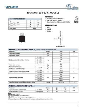
VBZL50N06 www.VBsemi.com N-Channel 30-V (D-S) MOSFET FEATURES TrenchFET Power MOSFET PRODUCT SUMMARY 100 % Rg and UIS Tested VDS 30 V Compliant to RoHS Directive 2011/65/EU RDS(on) VGS = 10 V 3 m RDS(on) VGS = 4.5 V 4 m APPLICATIONS ID 150 A OR-ing Configuration Single Server DC/DC D D2PAK (TO-263) G G D S S N-Channel MOSFET ABSOLUTE M... See More ⇒
suu50n06-07l.pdf
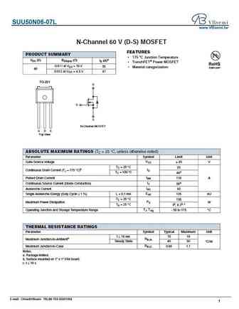
SUU50N06-07L www.VBsemi.tw N-Channel 60 V (D-S) MOSFET FEATURES PRODUCT SUMMARY 175 C Junction Temperature VDS (V) RDS(on) ( ) ID (A)a TrenchFET Power MOSFET 0.011 at VGS = 10 V 55 Material categorization 60 0.012 at VGS = 4.5 V 47 TO-251 D G S N-Channel MOSFET G D S Top View ABSOLUTE MAXIMUM RATINGS (TC = 25 C, unless otherwise noted) Parameter Sy... See More ⇒
sqd50n06-09l.pdf

SQD50N06-09L www.VBsemi.tw N-Channel 60 V (D-S) MOSFET FEATURES PRODUCT SUMMARY 175 C Junction Temperature VDS (V) RDS(on) ( ) ID (A)a TrenchFET Power MOSFET 0.012 at VGS = 10 V 50 Material categorization 60 0.013 at VGS = 4.5 V 45 D TO-252 G S G D S N-Channel MOSFET ABSOLUTE MAXIMUM RATINGS (TC = 25 C, unless otherwise noted) Parameter Symbol Lim... See More ⇒
yjp150n06aq.pdf
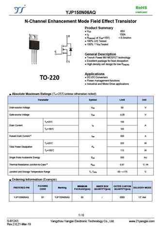
RoHS COMPLIANT YJP150N06AQ N-Channel Enhancement Mode Field Effect Transistor Product Summary V 60V DS I 150A D R ( at V =10V) 5.5mohm DS(ON) GS 100% UIS Tested 100% VDS Tested General Description Trench Power MV MOSFET technology Excellent package for heat dissipation High density cell design for low R DS(ON) Applications ... See More ⇒
yjb150n06bq.pdf
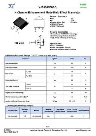
RoHS COMPLIANT YJB150N06BQ N-Channel Enhancement Mode Field Effect Transistor Product Summary V 60V DS I 150A D R ( at V =10V) 5.5mohm DS(ON) GS 100% UIS Tested 100% VDS Tested General Description Trench Power MV MOSFET technology Excellent package for heat dissipation High density cell design for low R DS(ON) Applications ... See More ⇒
hm50n06ka.pdf
N-Channel Enhancement Mode Power MOSFET Description The uses advanced trench technology and design to provide excellent RDS(ON) with low gate charge. It can be used in a wide variety of applications. General Features VDS =60V,ID =50A RDS(ON) ... See More ⇒
hm50n06i.pdf
HM50N06I N-Channel Enhancement Mode Power MOSFET Description The HM50N06I uses advanced trench technology and design to provide excellent RDS(ON) with low gate charge. It can be used in a wide variety of applications. General Features VDS =60V,ID =50A RDS(ON) ... See More ⇒
hm50n06.pdf
HM50N06 N-Channel Enhancement Mode Power MOSFET DESCRIPTION The HM50N06 uses advanced trench technology and design to provide excellent RDS(ON) with low gate charge. It can be used in a wide variety of applications. GENERAL FEATURES VDS =60V,ID =50A RDS(ON) ... See More ⇒
hm50n06d.pdf
HM50N06D N-Channel Enhancement Mode Power MOSFET Description The HM50N06D uses advanced trench technology and design to provide excellent RDS(ON) with low gate charge. It can be used in a wide variety of applications. General Features VDS = 60V,ID =50A RDS(ON) ... See More ⇒
hm50n06a.pdf
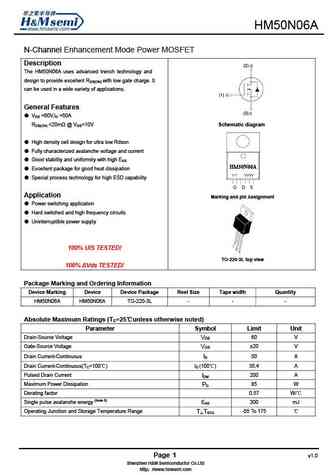
HM50N06A N-Channel Enhancement Mode Power MOSFET Description The HM50N06A uses advanced trench technology and design to provide excellent RDS(ON) with low gate charge. It can be used in a wide variety of applications. General Features VDS =60V,ID =50A RDS(ON) ... See More ⇒
hms150n06d.pdf
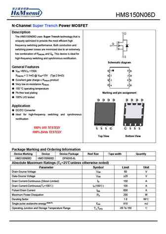
HMS150N06D N-Channel Super Trench Power MOSFET Description The HMS150N06D uses Super Trench technology that is uniquely optimized to provide the most efficient high frequency switching performance. Both conduction and switching power losses are minimized due to an extremely low combination of RDS(ON) and Qg. This device is ideal for high-frequency switching and synchronous recti... See More ⇒
hm50n06k.pdf
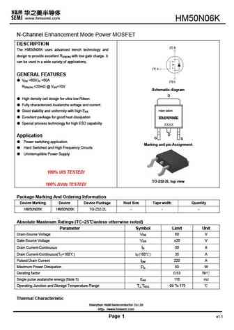
HM50N06K N-Channel Enhancement Mode Power MOSFET DESCRIPTION The HM50N06K uses advanced trench technology and design to provide excellent RDS(ON) with low gate charge. It can be used in a wide variety of applications. GENERAL FEATURES VDS =60V,ID =50A RDS(ON) ... See More ⇒
mpg50n06p.pdf
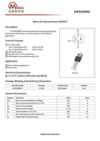
Silicon N-Channel Power MOSFET Description The MPG50N06 uses advanced trench technology and design to provide Excellent R . It can be used in a wide variety of DS(ON) applications. General Features V =60V,I =50A DS D R 14m @V =10V (Typ 11.0 m ) dson GS R 16m @V =4.5V (Typ 12.5m ) dson GS Low ON Resistance Low Reverse transfer capacitances 100% Single P... See More ⇒
mdt50n06d.pdf
60V N-Channel Power MOSFE Description The MDT50N06 uses advanced trench technology to provide excellent RDS(ON), low gate charge. It can be used in a wide variety of applications. General Features V =60V, R ... See More ⇒
mp50n06.pdf
Silicon N-Channel Power MOSFET Description The MP50N06 uses advanced trench technology and design to provide Excellent R . It can be used in a DS(ON) wide variety of applications. General Features Schematic diagram V =60V,I =50A DS D R 14m @V =10V (Typ 11.0 m ) dson GS R n 16m @V =4.5V (Typ 12.5m ) dso GS Low ON Resistance Low Reverse transfer capacitances ... See More ⇒
e50n06 d50n06 h50n06 t50n06.pdf
50N06 60V N-Channel Power MOSFET TO-263 TO-252 Features Low FOM RDS(on) Qgd 100% avalanche tested Easy to use/drive RoHS compliant TO-251 TO-220 Drain Applications DC/DC Converter Battery Protection Charge/Discharge Gate Load Switch Synchronous Rectification Source Key Performance Parameters Parameter Value Unit VDS@ Tc=25 60 V RDS(on),... See More ⇒
phd50n06lt.pdf
Isc N-Channel MOSFET Transistor PHD50N06LT FEATURES With To-252(DPAK) package Low input capacitance and gate charge Low gate input resistance 100% avalanche tested Minimum Lot-to-Lot variations for robust device performance and reliable operation APPLICATIONS Switching applications ABSOLUTE MAXIMUM RATINGS(T =25 ) a SYMBOL PARAMETER VALUE UNIT V Drain-Source Vol... See More ⇒
ipd350n06l.pdf
isc N-Channel MOSFET Transistor IPD350N06L,IIPD350N06L FEATURES Static drain-source on-resistance RDS(on) 35m Enhancement mode 100% avalanche tested Minimum Lot-to-Lot variations for robust device performance and reliable operation DESCRITION Fast switching ABSOLUTE MAXIMUM RATINGS(T =25 ) a SYMBOL PARAMETER VALUE UNIT V Drain-Source Voltage 60 V DSS V Ga... See More ⇒
mtp50n06v.pdf
INCHANGE Semiconductor isc Product Specification isc N-Channel MOSFET Transistor MTP50N06V FEATURES Drain Current ID=42A@ TC=25 Drain Source Voltage- VDSS= 60V(Min) Static Drain-Source On-Resistance RDS(on) = 0.028 (Max) DESCRIPTION Designed for low voltage, high speed switching applications in power supplies, converters and power motor controls, these ... See More ⇒
rfp50n06.pdf
isc N-Channel MOSFET Transistor RFP50N06 DESCRIPTION Drain Current I =50A@ T =25 D C Drain Source Voltage- V =60V(Min) DSS Static Drain-Source On-Resistance R = 22m (Max) DS(on) Fast Switching Speed Minimum Lot-to-Lot variations for robust device performance and reliable operation APPLICATIONS Designed for use in applications such as swithing Regulators,switc... See More ⇒
fqd50n06.pdf
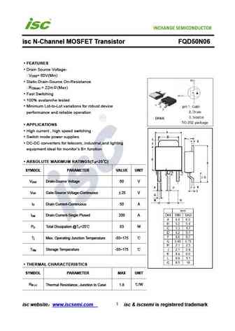
isc N-Channel MOSFET Transistor FQD50N06 FEATURES Drain Source Voltage- V = 60V(Min) DSS Static Drain-Source On-Resistance R = 22m (Max) DS(on) Fast Switching 100% avalanche tested Minimum Lot-to-Lot variations for robust device performance and reliable operation APPLICATIONS High current , high speed switching Switch mode power supplies DC-DC converters ... See More ⇒
fqpf50n06.pdf
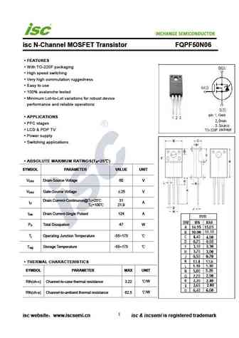
INCHANGE Semiconductor isc N-Channel MOSFET Transistor FQPF50N06 FEATURES With TO-220F packaging High speed switching Very high commutation ruggedness Easy to use 100% avalanche tested Minimum Lot-to-Lot variations for robust device performance and reliable operationz APPLICATIONS PFC stages LCD & PDP TV Power supply Switching applications ABSOLUTE MAXIM... See More ⇒
fqp50n06l.pdf
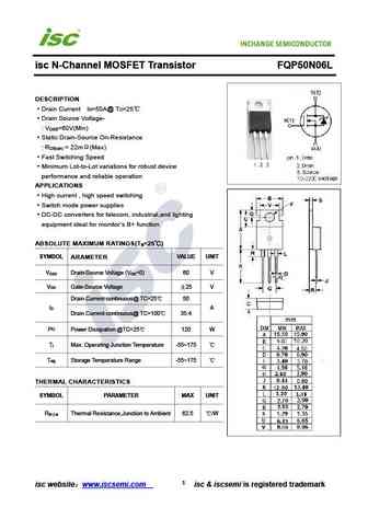
isc N-Channel MOSFET Transistor FQP50N06L DESCRIPTION Drain Current I =50A@ T =25 D C Drain Source Voltage- V =60V(Min) DSS Static Drain-Source On-Resistance R = 22m (Max) DS(on) Fast Switching Speed Minimum Lot-to-Lot variations for robust device performance and reliable operation APPLICATIONS High current , high speed switching Switch mode power supplies ... See More ⇒
50n06fi.pdf
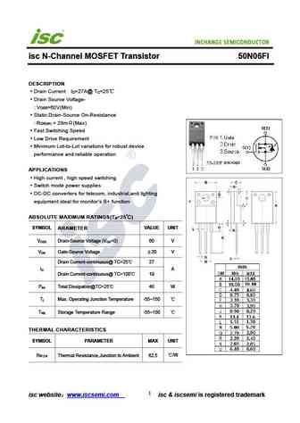
isc N-Channel MOSFET Transistor 50N06FI DESCRIPTION Drain Current I =27A@ T =25 D C Drain Source Voltage- V =60V(Min) DSS Static Drain-Source On-Resistance R = 28m (Max) DS(on) Fast Switching Speed Low Drive Requirement Minimum Lot-to-Lot variations for robust device performance and reliable operation APPLICATIONS High current , high speed switching Switc... See More ⇒
150n06y.pdf
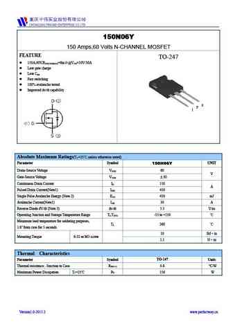
150N06Y 150 Amps,60 Volts N-CHANNEL MOSFET FEATURE TO-247 150A,60V,R =6m @V =10V/30A DS(ON)MAX GS Low gate charge Low C iss Fast switching 100% avalanche tested Improved dv/dt capability Absolute Maximum Ratings(T =25 ,unless otherwise noted) C Parameter Symbol UNIT 150N06Y Drain-Source Voltage V 60 DSS V Gate-Source Voltage V 30 GSS Continuous ... See More ⇒
ap50n06nf.pdf
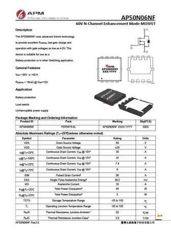
AP50N06NF 60V N-Channel Enhancement Mode MOSFET Description The AP50N06NF uses advanced trench technology to provide excellent R , low gate charge and DS(ON) operation with gate voltages as low as 4.5V. This device is suitable for use as a Battery protection or in other Switching application. General Features V = 60V I =50 A DS D R ... See More ⇒
ap50n06p ap50n06t.pdf
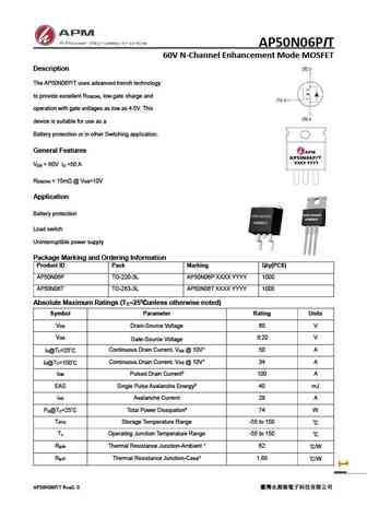
AP50N06PIT 60V N-Channel Enhancement Mode MOSFET Description The AP50N06P/T uses advanced trench technology to provide excellent R , low gate charge and DS(ON) operation with gate voltages as low as 4.5V. This device is suitable for use as a Battery protection or in other Switching application. General Features V = 60V I =50 A DS D R ... See More ⇒
ap50n06bd ap50n06by.pdf
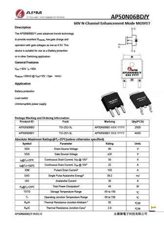
AP50N06BDIY 60V N-Channel Enhancement Mode MOSFET Description The AP50N06BD/Y uses advanced trench technology to provide excellent R , low gate charge and DS(ON) operation with gate voltages as low as 4.5V. This device is suitable for use as a Battery protection or in other Switching application. General Features V = 60V I =50A DS D R ... See More ⇒
ap50n06d.pdf
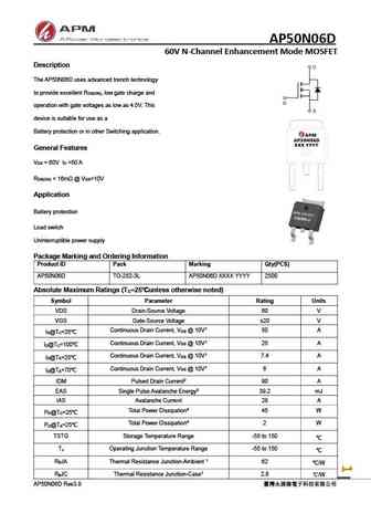
AP50N06D 60V N-Channel Enhancement Mode MOSFET Description The AP50N06D uses advanced trench technology to provide excellent R , low gate charge and DS(ON) operation with gate voltages as low as 4.5V. This device is suitable for use as a Battery protection or in other Switching application. General Features V = 60V I =50 A DS D R ... See More ⇒
ap50n06df.pdf
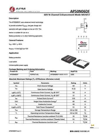
AP50N06DF 60V N-Channel Enhancement Mode MOSFET Description The AP50N06DF uses advanced trench technology to provide excellent R , low gate charge and DS(ON) operation with gate voltages as low as 4.5V. This device is suitable for use as a Battery protection or in other Switching application. General Features V = 60V I =50 A DS D R ... See More ⇒
ap50n06y.pdf
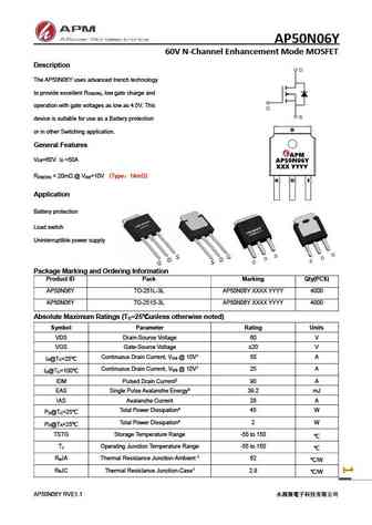
AP50N06Y 60V N-Channel Enhancement Mode MOSFET Description The AP50N06Y uses advanced trench technology to provide excellent R , low gate charge and DS(ON) operation with gate voltages as low as 4.5V. This device is suitable for use as a Battery protection or in other Switching application. General Features V =60V I =50A DS D R ... See More ⇒
Detailed specifications: 15N06, 12N10, 15N20, 19N10, 22N20, 25N06, 25N10, 30N06, IRFB7545, 60N06, 60N08, 6N10, 70N06, 75N75, 7N10, 7N10Z, 80N08
Keywords - 50N06 MOSFET specs
50N06 cross reference
50N06 equivalent finder
50N06 pdf lookup
50N06 substitution
50N06 replacement
Learn how to find the right MOSFET substitute. A guide to cross-reference, check specs and replace MOSFETs in your circuits.
