MTP2010J3 Specs and Replacement
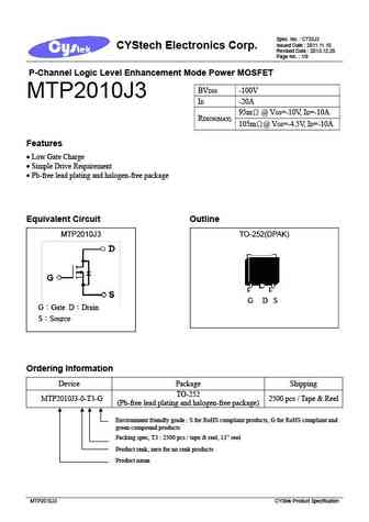
Type Designator: MTP2010J3
Type of Transistor: MOSFET
Type of Control Channel: P-Channel
Absolute Maximum Ratings
Pd ⓘ - Maximum Power Dissipation: 50 W
|Vds|ⓘ - Maximum Drain-Source Voltage: 100 V
|Vgs|ⓘ - Maximum Gate-Source Voltage: 20 V
|Id| ⓘ - Maximum Drain Current: 20 A
Tj ⓘ - Maximum Junction Temperature: 175 °C
Electrical Characteristics
tr ⓘ - Rise Time: 5 nS
Cossⓘ - Output Capacitance: 91 pF
RDSonⓘ - Maximum Drain-Source On-State Resistance: 0.086 Ohm
Package: TO-252
MTP2010J3 substitution
- MOSFET ⓘ Cross-Reference Search
MTP2010J3 datasheet
mtp2010j3.pdf
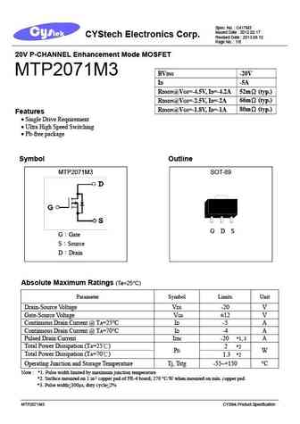
Spec. No. C732J3 Issued Date 2011.11.10 CYStech Electronics Corp. Revised Date 2013.12.26 Page No. 1/9 P-Channel Logic Level Enhancement Mode Power MOSFET BVDSS -100V MTP2010J3 ID -20A 95m @ VGS=-10V, ID=-10A RDSON(MAX) 105m @ VGS=-4.5V, ID=-10A Features Low Gate Charge Simple Drive Requirement Pb-free lead plating and halogen-free package E... See More ⇒
mtp20n06v.pdf
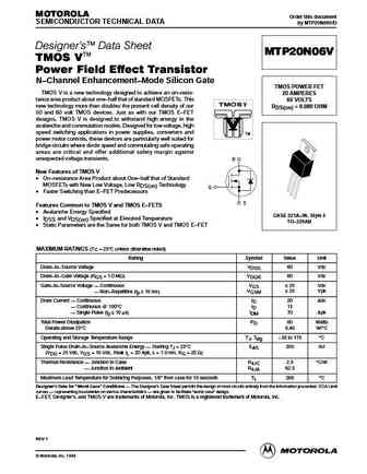
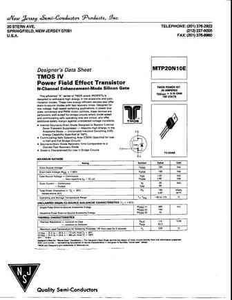
MOTOROLA Order this document SEMICONDUCTOR TECHNICAL DATA by MTP20N06V/D Designer's Data Sheet MTP20N06V TMOS V Power Field Effect Transistor N Channel Enhancement Mode Silicon Gate TMOS POWER FET TMOS V is a new technology designed to achieve an on resis- 20 AMPERES tance area product about one half that of standard MOSFETs. This 60 VOLTS new technology more than ... See More ⇒
mtp20n20e.pdf
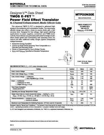
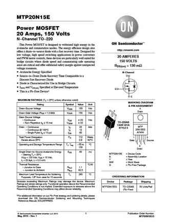
MOTOROLA Order this document SEMICONDUCTOR TECHNICAL DATA by MTP20N20E/D Designer's Data Sheet MTP20N20E TMOS E-FET. Motorola Preferred Device Power Field Effect Transistor N Channel Enhancement Mode Silicon Gate TMOS POWER FET This advanced TMOS E FET is designed to withstand high 20 AMPERES energy in the avalanche and commutation modes. The new energy 200 VOLTS effi... See More ⇒
mtp20n20erev2x.pdf
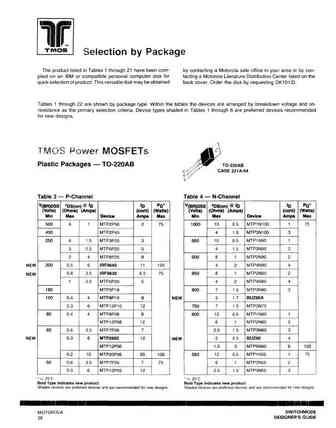
MOTOROLA Order this document SEMICONDUCTOR TECHNICAL DATA by MTP20N20E/D Designer's Data Sheet MTP20N20E TMOS E-FET. Motorola Preferred Device Power Field Effect Transistor N Channel Enhancement Mode Silicon Gate TMOS POWER FET This advanced TMOS E FET is designed to withstand high 20 AMPERES energy in the avalanche and commutation modes. The new energy 200 VOLTS effi... See More ⇒
Detailed specifications: MTNN8453KQ8, MTP1013C3, MTP1013S3, MTP1067C6, MTP1406J3, MTP1406L3, MTP1406M3, MTP162M3, AO4468, MTP2071M3, MTP2301N3, MTP2301S3, MTP2303N3, MTP2305N3, MTP2311M3, MTP2311N3, MTP2311V8
Keywords - MTP2010J3 MOSFET specs
MTP2010J3 cross reference
MTP2010J3 equivalent finder
MTP2010J3 pdf lookup
MTP2010J3 substitution
MTP2010J3 replacement
Can't find your MOSFET? Learn how to find a substitute transistor by analyzing voltage, current and package compatibility
History: STB16NM50N
🌐 : EN ES РУ
LIST
Last Update
MOSFET: AUW033N08BG | AUW025N10 | AUR030N10 | AUR020N10 | AUR020N085 | AUR014N10 | AUP074N10 | AUP065N10 | AUP062N08BG | AUP060N08AG
Popular searches
2sk1058 | ss8550 | mje15033 | 2sc945 datasheet | a92 transistor | rfp50n06 | bd140 datasheet | tip2955
