AO3400A Datasheet. Specs and Replacement
Type Designator: AO3400A 📄📄
Type of Transistor: MOSFET
Type of Control Channel: N-Channel
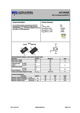
Absolute Maximum Ratings
Pd ⓘ - Maximum Power Dissipation: 1.4 W
|Vds|ⓘ - Maximum Drain-Source Voltage: 30 V
|Vgs|ⓘ - Maximum Gate-Source Voltage: 12 V
|Id| ⓘ - Maximum Drain Current: 5.7 A
Tj ⓘ - Maximum Junction Temperature: 150 °C
Electrical Characteristics
tr ⓘ - Rise Time: 2.5 nS
Cossⓘ - Output Capacitance: 75 pF
RDSonⓘ - Maximum Drain-Source On-State Resistance: 0.0265 Ohm
Package: SOT23
📄📄 Copy
- MOSFET ⓘ Cross-Reference Search
AO3400A datasheet
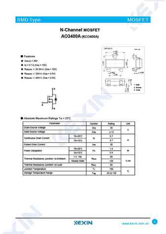
..2. Size:1866K kexin
ao3400a.pdf 
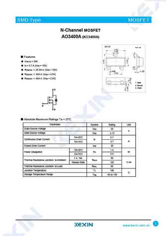
SMD Type MOSFET N-Channel MOSFET AO3400A (KO3400A) SOT-23 Unit mm +0.1 2.9 -0.1 0.4+0.1 -0.1 3 Features VDS (V) = 30V ID = 5.7 A (VGS = 10V) 1 2 RDS(ON) 26.5m (VGS = 10V) +0.1 +0.05 0.95 -0.1 0.1 -0.01 +0.1 1.9 -0.1 RDS(ON) 32m (VGS = 4.5V) RDS(ON) 48m (VGS = 2.5V) 1. Gate 2. Source 3. Drain D D G G S S Absolute... See More ⇒
..3. Size:1508K umw-ic
ao3400a.pdf
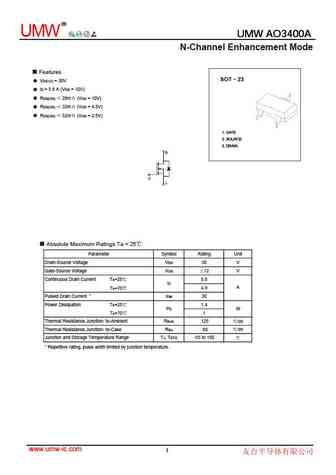
R UMW UMW AO3400A UMW AO3400A N-Channel Enhancement Mode Features SOT 23 VDS (V) = 30V ID = 5.8 A (VGS = 10V) RDS(ON) 28m (VGS = 10V) RDS(ON) 33m (VGS = 4.5V) RDS(ON) 52m (VGS = 2.5V) 1. GATE 2. SOURCE 3. DRAIN Absolute Maximum Ratings Ta = 25 Parameter Symbol Rating Unit Drain-Source Voltage VDS 30 V Gate-Source Voltage VGS 12 V Continuous Drain Current TA=25 5.8 ID ... See More ⇒
..4. Size:2049K born
ao3400a.pdf
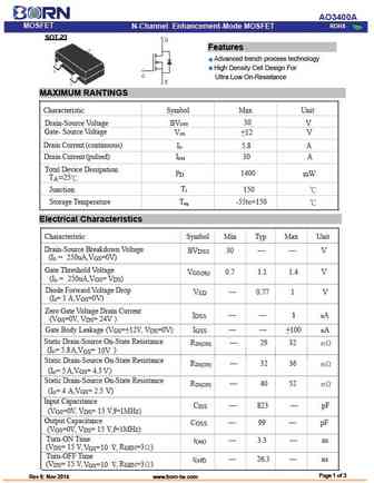
AO3400A MOSFET ROHS N-Channel Enhancement-Mode MOSFET SOT-23 - Features Advanced trench process technology High Density Cell Design For Ultra Low On-Resistance MAXIMUM RANTINGS Characteristic Symbol Max Unit Drain-Source Voltage BV 30 V DSS Gate- Source Voltage V +12 V GS Drain Current (continuous) 5.8 A I D Drain Current (pulsed) I 30 A DM Total Device Dissipat... See More ⇒
..5. Size:407K huashuo
ao3400a.pdf
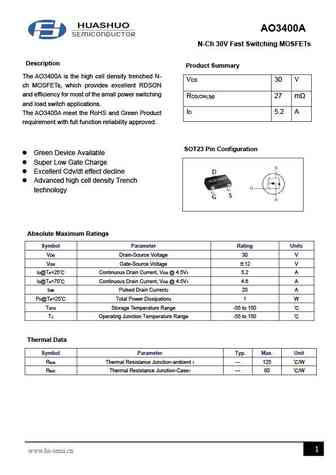
AO3400A N-Ch 30V Fast Switching MOSFETs Description Product Summary The AO3400A is the high cell density trenched N- VDS 30 V ch MOSFETs, which provides excellent RDSON and efficiency for most of the small power switching RDS(ON),typ 27 m and load switch applications. ID 5.2 A The AO3400A meet the RoHS and Green Product requirement with full function reliability approve... See More ⇒
0.1. Size:1871K kexin
ao3400a-3.pdf
SMD Type MOSFET N-Channel MOSFET AO3400A (KO3400A) SOT-23-3 Unit mm +0.2 2.9 -0.1 +0.1 0.4-0.1 3 Features VDS (V) = 30V ID = 5.7 A (VGS = 10V) RDS(ON) 26.5m (VGS = 10V) 1 2 +0.02 +0.1 0.15 -0.02 0.95 -0.1 RDS(ON) 32m (VGS = 4.5V) +0.1 1.9 -0.2 RDS(ON) 48m (VGS = 2.5V) 1. Gate 2. Source D D 3. Drain G G S S Absol... See More ⇒
8.1. Size:1848K htsemi
ao3400.pdf
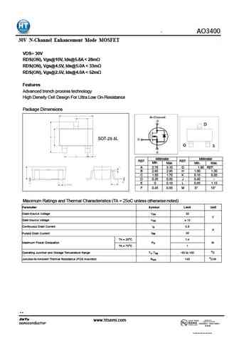
AO3400 30V N-Channel Enhancement Mode MOSFET VDS= 30V RDS(ON), Vgs@10V, Ids@5.8A ... See More ⇒
8.2. Size:2141K lge
ao3400.pdf
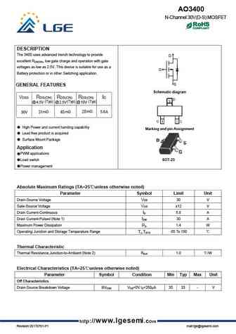
AO3400 N-Channel 30V(D-S) MOSFET DESCRIPTION The 3400 uses advanced trench technology to provide D excellent RDS(ON), low gate charge and operation with gate voltages as low as 2.5V. This device is suitable for use as a G Battery protection or in other Switching application. S GENERAL FEATURES Schematic diagram VDSS RDS(ON) RDS(ON) RDS(ON) ID @ 4.5V (Typ) @ 2.5V (Typ) @ 1... See More ⇒
8.3. Size:342K aosemi
ao3400c.pdf
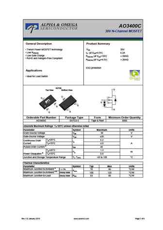
AO3400C 30V N-Channel MOSFET General Description Product Summary VDS Trench Power MOSFET technology 30V Low RDS(ON) ID (at VGS=4.5V) 6.2A Low Gate Charge RDS(ON) (at VGS=10V) ... See More ⇒
8.4. Size:472K aosemi
ao3400.pdf
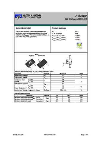
AO3400 30V N-Channel MOSFET General Description Product Summary VDS 30V The AO3400 combines advanced trench MOSFET technology with a low resistance package to provide ID (at VGS=10V) 5.8A extremely low RDS(ON). This device is suitable for use as a RDS(ON) (at VGS=10V) ... See More ⇒
8.5. Size:1266K shenzhen
ao3400.pdf
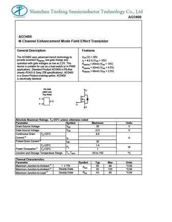
Shenzhen Tuofeng Semiconductor Technology Co., Ltd AO3400 AO3400 N-Channel Enhancement Mode Field Effect Transistor General Description Features The AO3400 uses advanced trench technology to VDS (V) = 30V provide excellent RDS(ON), low gate charge and ID = 4.8 A (VGS = 10V) operation with gate voltages as low as 2.5V. This RDS(ON) ... See More ⇒
8.6. Size:781K blue-rocket-elect
ao3400.pdf
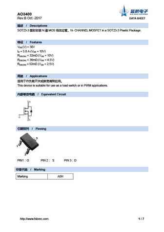
AO3400 Rev.B Oct.-2017 DATA SHEET / Descriptions SOT23-3 N MOS N- CHANNEL MOSFET in a SOT23-3 Plastic Package. / Features VDS (V) = 30V ID = 5.8 A (VGS = 10V) RDS(ON) ... See More ⇒
8.7. Size:53K kexin
ko3400 ao3400.pdf
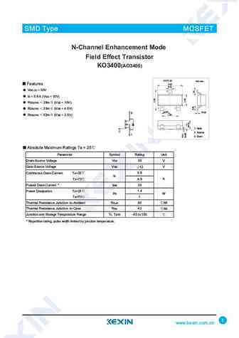
SMD Type IC SMD Type MOSFET N-Channel Enhancement Mode Field Effect Transistor KO3400(AO3400) SOT-23 Unit mm +0.1 Features 2.9-0.1 +0.1 0.4-0.1 VDS (V) = 30V 3 ID =5.8 A(VGS =10V) RDS(ON) 28m (VGS = 10V) 12 RDS(ON) 33m (VGS =4.5V) +0.1 +0.05 0.95-0.1 0.1-0.01 +0.1 1.9-0.1 RDS(ON) 52m (VGS =2.5V) 1.Base 1. Gate 2.Emitter 2. Source 3. Drain 3.collector Absolute Maxim... See More ⇒
8.8. Size:1190K kexin
ao3400-3.pdf
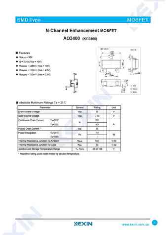
SMD Type IC SMD Type MOSFET N-Channel Enhancement MOSFET AO3400 (KO3400) SOT-23-3 Unit mm +0.2 2.9 -0.1 Features +0.1 0.4-0.1 3 VDS (V) = 30V ID = 5.8 A (VGS = 10V) RDS(ON) 28m (VGS = 10V) 1 2 RDS(ON) 33m (VGS = 4.5V) +0.02 +0.1 0.15 -0.02 0.95 -0.1 RDS(ON) 52m (VGS = 2.5V) D +0.1 1.9 -0.2 1. Gate 2. Source G S 3. Drain Absolute Maximum Ratings Ta = 25 Parameter Sy... See More ⇒
8.9. Size:1115K kexin
ao3400.pdf
SMD Type IC SMD Type MOSFET N-Channel Enhancement Mode Field Effect Transistor AO3400 (KO3400) SOT-23 Unit mm +0.1 Features 2.9 -0.1 +0.1 0.4 -0.1 VDS (V) = 30V 3 ID = 5.8 A (VGS = 10V) RDS(ON) 28m (VGS = 10V) 1 2 RDS(ON) 33m (VGS = 4.5V) +0.1 +0.05 0.95 -0.1 0.1 -0.01 +0.1 1.9 -0.1 RDS(ON) 52m (VGS = 2.5V) 1.Base 1. Gate 2.Emitter 2. Source 3. Drain 3.collector Ab... See More ⇒
8.10. Size:1208K born
ao3400.pdf
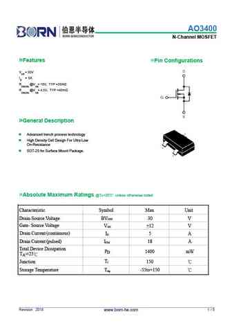
AO3400 N-Channel MOSFET Features Pin Configurations V = 30V DS I D = 5A R @V = 10V, TYP =35m DS(ON) GS R @V = 4.5V, TYP =40m DS(ON) GS General Description Advanced trench process technology High Density Cell Design For Ultra Low On-Resistance SOT-23 for Surface Mount Package. Absolute Maximum Ratings @T =25 unless otherwise noted A Characteri... See More ⇒
8.11. Size:591K guangdong hottech
ao3400.pdf
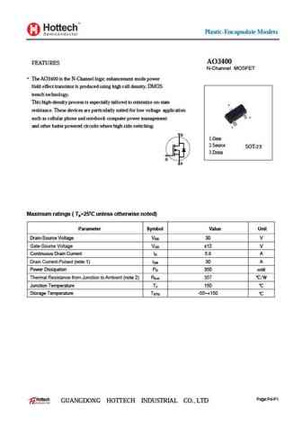
Plastic-Encapsulate Mosfets AO3400 FEATURES N-Channel MOSFET The AO3400 is the N-Channel logic enhancement mode power field effect transistor is produced using high cell density, DMOS trench technology. This high-density process is especially tailored to minimize on-state resistance. These devices are particularly suited for low voltage application such as cellular phone and notebook c... See More ⇒
8.12. Size:602K msksemi
ao3400mi-ms.pdf
www.msksemi.com AO3400MI-MS Semiconductor Compiance SOT-23 FEATURE High dense cell design for extremely low R DS(ON) Exceptional on-resistance and maximum DC current capability 1. GATE 2. SOURCE APPLICATION 3. DRAIN Load/Power Switching Interfacing Switching Equivalent Circuit I V(BR)DSS RDS(on)MAX D 35m @ 10V 40m @4.5V 30 V 5.8A 52m @2.5V Maximum ratin... See More ⇒
8.13. Size:1535K cn puolop
ao3400.pdf
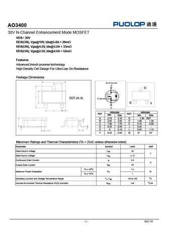
AO3400 30V N-Channel Enhancement Mode MOSFET VDS= 30V RDS(ON), Vgs@10V, Ids@5.8A ... See More ⇒
8.14. Size:656K cn shikues
ao3400.pdf
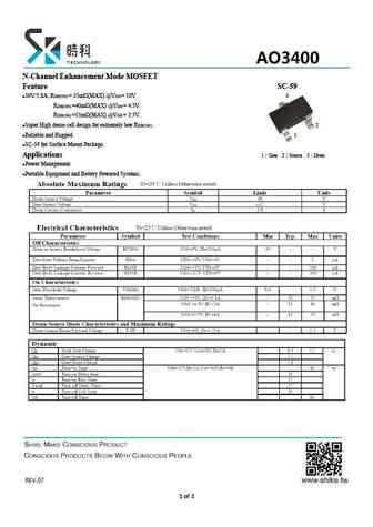
N-Channel Enhancement Mode MOSFET Feature SC-59 30V/5.8A, RDS(ON) = 35m (MAX) @VGS = 10V. 3 RDS(ON) =40m (MAX) @VGS = 4.5V. RDS(ON) =55m (MAX) @VGS = 2.5V. Super High dense cell design for extremely low RDS(ON) . 2 Reliable and Rugged. 1 SC-59 for Surface Mount Package. Applications 1 Gate 2 Source 3 Drain Power Management Portable Equipment and... See More ⇒
8.15. Size:1027K cn alj
ao3400.pdf
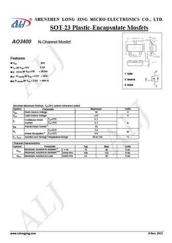
SHENZHEN LONG JING MICRO-ELECTRONICS CO., LTD. SOT-23 Plastic-Encapsulate Mosfets AO3400 N-Channel Mosfet Features 30V VDS 5.7A I (at VGS=10V D (at VGS=10V ... See More ⇒
8.16. Size:1973K cn twgmc
ao3400.pdf
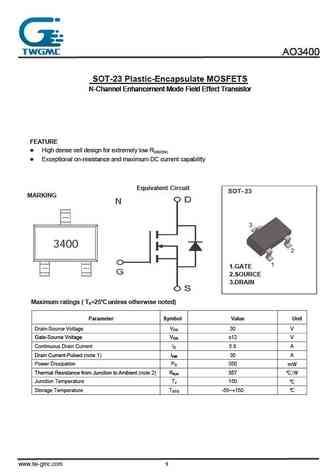
AO3400 AO3400 AO3400 AO3400 SI2305 SOT-23 Plastic-Encapsulate MOSFETS N-Channel Enhancement Mode Field Effect Transistor N-Channel Enhancement Mode Field Effect Transistor N-Channel Enhancement Mode Field Effect Transistor N-Channel Enhancement Mode Field Effect Transistor AO3400 AO3400 AO3400 AO3400 AO3400 FEATURE High dense cell design for extremely low RDS(ON) Excepti... See More ⇒
8.17. Size:849K cn vbsemi
ao3400.pdf
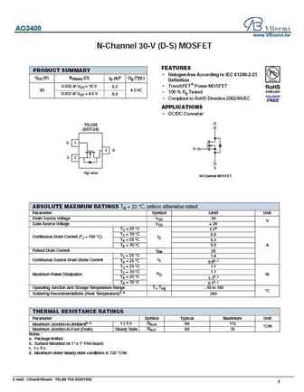
AO3400 www.VBsemi.tw N-Channel 30-V (D-S) MOSFET FEATURES PRODUCT SUMMARY Halogen-free According to IEC 61249-2-21 VDS (V) RDS(on) ( ) ID (A)a Qg (Typ.) Definition 0.030 at VGS = 10 V TrenchFET Power MOSFET 6.5 30 4.5 nC 100 % Rg Tested 0.033 at VGS = 4.5 V 6.0 Compliant to RoHS Directive 2002/95/EC APPLICATIONS DC/DC Converter D TO-236 (SOT-23) G 1... See More ⇒
8.19. Size:557K cn minos
ao3400s.pdf
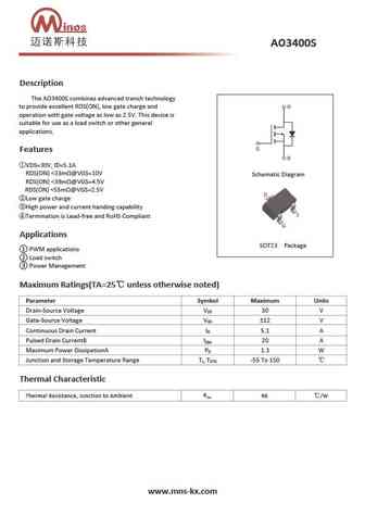
Description The AO3400S combines advanced trench technology to provide excellent RDS(ON), low gate charge and operation with gate voltage as low as 2.5V. This device is suitable for use as a load switch or other general applications. Features VDS=30V, ID=5.1A RDS(ON) ... See More ⇒
Detailed specifications: MTP9575J3, MTP9575L3, MTP9575Q8, MTP9620Q8, MTP9620V8, MTS3572G6, AO3160, AO3162, 4N60, AO3402, AO3403, AO3404, AO3404A, AO3406, AO3407A, AO3409, AO3413
Keywords - AO3400A MOSFET specs
AO3400A cross reference
AO3400A equivalent finder
AO3400A pdf lookup
AO3400A substitution
AO3400A replacement
Step-by-step guide to finding a MOSFET replacement. Cross-reference parts and ensure compatibility for your repair or project.